CY62157CV30/33
Document #: 38-05014 Rev. *F Page 6 of 13
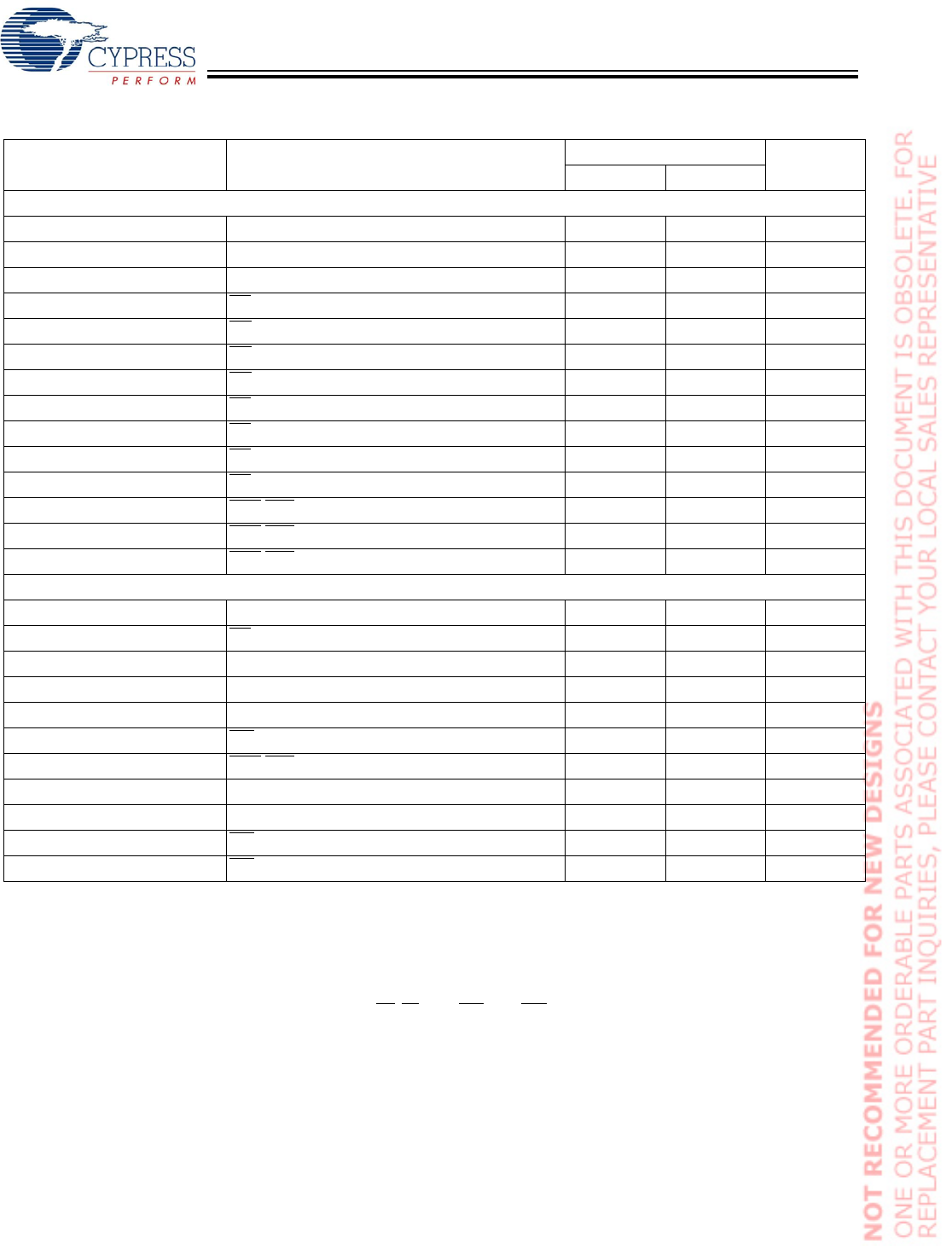
Switching Characteristics Over the Operating Range
[10]
Parameter Description
70 ns
UnitMin. Max.
Read Cycle
t
RC
Read Cycle Time 70 ns
t
AA
Address to Data Valid 70 ns
t
OHA
Data Hold from Address Change 10 ns
t
ACE
CE
1
LOW and CE
2
HIGH to Data Valid 70 ns
t
DOE
OE LOW to Data Valid 35 ns
t
LZOE
OE LOW to Low-Z
[11]
5ns
t
HZOE
OE HIGH to High-Z
[11, 12]
25 ns
t
LZCE
CE
1
LOW and CE
2
HIGH to Low-Z
[11]
10 ns
t
HZCE
CE
1
HIGH or CE
2
LOW to High-Z
[11, 12]
25 ns
t
PU
CE
1
LOW and CE
2
HIGH to Power-up 0 ns
t
PD
CE
1
HIGH or CE
2
LOW to Power-down 70 ns
t
DBE
BHE/BLE LOW to Data Valid 70 ns
t
LZBE
[11]
BHE/BLE LOW to Low-Z
[13]
5ns
t
HZBE
BHE/BLE HIGH to High-Z
[11, 12]
25 ns
Write Cycle
[14]
t
WC
Write Cycle Time 70 ns
t
SCE
CE
1
LOW and CE
2
HIGH to Write End 60 ns
t
AW
Address Set-up to Write End 60 ns
t
HA
Address Hold from Write End 0 ns
t
SA
Address Set-up to Write Start 0 ns
t
PWE
WE Pulse Width 50 ns
t
BW
BHE/BLE Pulse Width 60 ns
t
SD
Data Set-up to Write End 30 ns
t
HD
Data Hold from Write End 0 ns
t
HZWE
WE LOW to High-Z
[11, 12]
25 ns
t
LZWE
WE HIGH to Low-Z
[11]
5ns
Notes:
10.Test conditions assume signal transition time of 5 ns or less, timing reference levels of V
CC(typ.)
/2, input pulse levels of 0 to V
CC(typ.)
, and output loading of the
specified I
OL
/I
OH
and 30-pF load capacitance.
11.At any given temperature and voltage condition, t
HZCE
is less than t
LZCE
, t
HZBE
is less than t
LZBE
, t
HZOE
is less than t
LZOE
, and t
HZWE
is less than t
LZWE
for any
given device.
12.t
HZOE
, t
HZCE
, t
HZBE
, and t
HZWE
transitions are measured when the outputs enter a high-impedance state.
13.When both byte enables are toggled together this value is 10 ns.
14.The internal Write time of the memory is defined by the overlap of WE
, CE
1
= V
IL
, BHE and/or BLE = V
IL
, CE
2
= V
IH
. All signals must be ACTIVE to initiate a
Write and any of these signals can terminate a Write by going INACTIVE. The data input set-up and hold timing should be referenced to the edge of the signal
that terminates the Write.
[+] Feedback


