DM9161B
10/100 Mbps Fast Ethernet Physical Layer Single Chip Transceiver
25 Final
Version: DM9161B-12-DS-F01
January 31, 2008
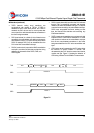
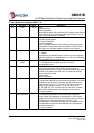
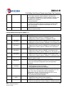
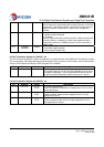
0 = Link is not established
The link status bit is implemented with a latching function, so that the
occurrence of a link failure condition causes the link status bit to be
cleared and remain cleared until it is read via the management
interface
1.1 Jabber detect 0, RO/LH
Jabber Detect
1 = Jabber condition detected
0 = No jabber
This bit is implemented with a latching function. Jabber conditions will
set this bit unless it is cleared by a read to this register through a
management interface or a DM9161B reset. This bit works only in
10Mbps mode
1.0 Extended
capability
1,RO/P
Extended Capability
1 = Extended register capable
0 = Basic register capable only
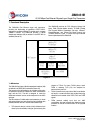
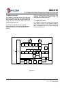
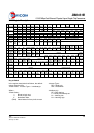
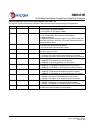
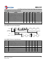
8.3 PHY ID Identifier Register #1 (PHYID1) - 02
The PHY Identifier Registers #1 and #2 work together in a single identifier of the DM9161B. The Identifier consists
of a concatenation of the Organizationally Unique Identifier (OUI), a vendor's model number, and a model revision
number. DAVICOM Semiconductor's IEEE assigned OUI is 00606E.
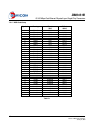
Bit Bit Name Default Description
2.15-2.0 OUI_MSB <0181h> OUI Most Significant Bits
This register stores bit 3 to 18 of the OUI (00606E) to bit 15 to 0 of
this register respectively. The most significant two bits of the OUI
are ignored (the IEEE standard refers to these as bit 1 and 2)
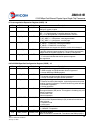
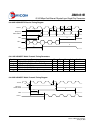
8.4 PHY ID Identifier Register #2 (PHYID2) - 03
Bit Bit Name Default Description
3.15-3.10 OUI_LSB <101110>,
RO/P
OUI Least Significant Bits
Bit 19 to 24 of the OUI (00606E) are mapped to bit 15 to 10 of this
register respectively
3.9-3.4 VNDR_MDL <001011>,
RO/P
Vendor Model Number
Five bits of vendor model number mapped to bit 9 to 4 (most
significant bit to bit 9)
3.3-3.0 MDL_REV <0000>,
RO/P
Model Revision Number
Five bits of vendor model revision number mapped to bit 3 to 0
(most significant bit to bit 4)