2002 Oct 23 7
Philips Semiconductors Product specification
40 Msps, 10-bit analog-to-digital
interface for CCD cameras
TDA8783
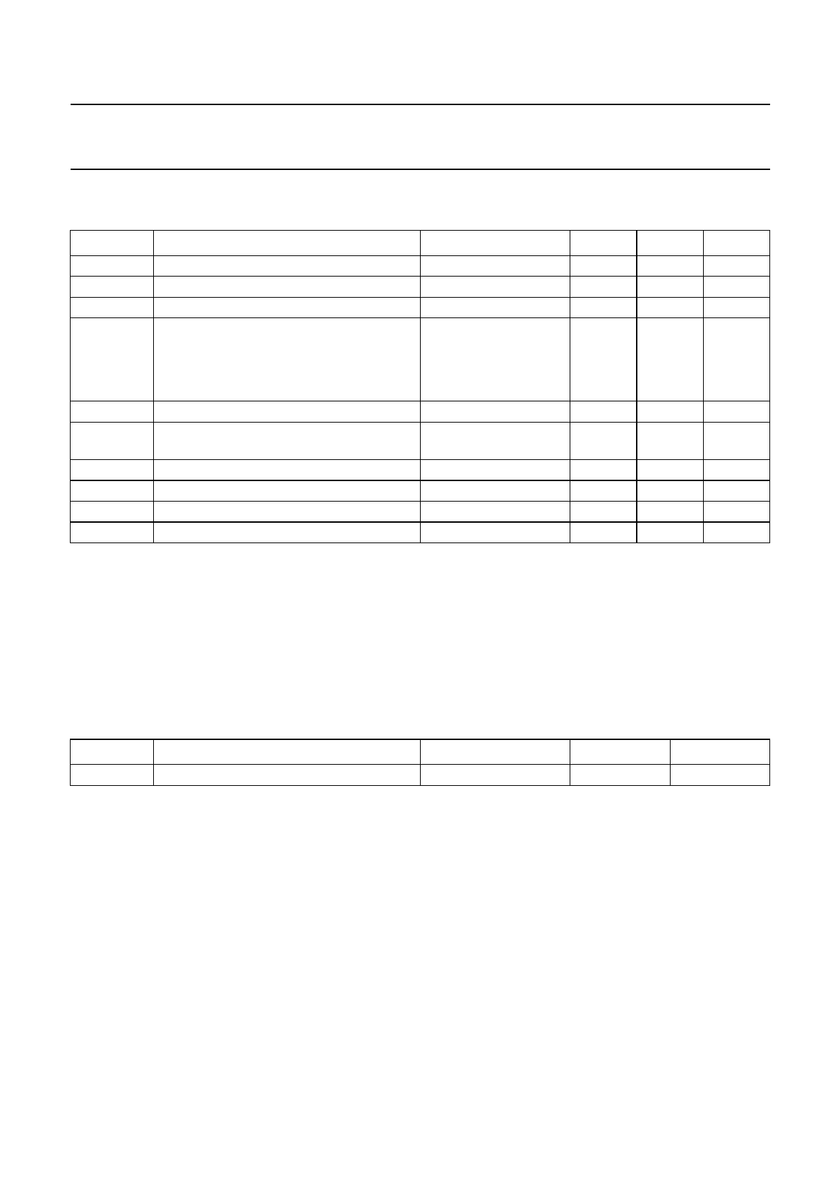
LIMITING VALUES
In accordance with the Absolute Maximum Rating System (IEC 60134).
Note
1. The supply voltages V
CCA
, V
CCD
and V
CCO
may have any value between −0.3 and +7.0 V provided that the supply
voltage difference ∆V
CC
remains as indicated.
HANDLING
Inputs and outputs are protected against electrostatic discharges in normal handling. However, to be totally safe, it is
desirable to take normal precautions appropriate to handling integrated circuits.
THERMAL CHARACTERISTICS
SYMBOL PARAMETER CONDITIONS MIN. MAX. UNIT
V
CCA
analog supply voltage note 1 −0.3 +7.0 V
V
CCD
digital supply voltage note 1 −0.3 +7.0 V
V
CCO
output stages supply voltage note 1 −0.3 +7.0 V
∆V
CC
supply voltage difference
between V
CCA
and V
CCD
−1.0 +1.0 V
between V
CCA
and V
CCO
−1.0 +4.0 V
between V
CCD
and V
CCO
−1.0 +4.0 V
V
i
input voltage referenced to AGND −0.3 +7.0 V
V
CLK(p-p)
AC input voltage for switching
(peak-to-peak value)
referenced to DGND − V
CCD
V
I
o
output current − 10 mA
T
stg
storage temperature −55 +150 °C
T
amb
ambient temperature −20 +75 °C
T
j
junction temperature − 150 °C
SYMBOL PARAMETER CONDITIONS VALUE UNIT
R
th(j-a)
thermal resistance from junction to ambient in free air 76 K/W


