


AD9843A
–12–
REV. 0
2dB TO 36dB
CLPDM
CCDIN
10
DIGITAL
FILTERING
CLPOB
DC RESTORE
INPUT OFFSET
CLAMP
OPTICAL BLACK
CLAMP
0 TO 64 LSB
0.1F
DOUT
10-BIT
ADC
VGA
8-BIT
DAC
8
VGA GAIN
REGISTER
10
CDS
–2dB TO +10dB
INTERNAL
V
REF
2V FULL SCALE
CDS GAIN
REGISTER
6
CLAMP LEVEL
REGISTER
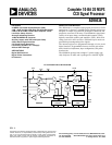
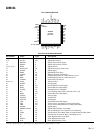
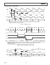
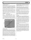
Figure 11. CCD-Mode Block Diagram
CIRCUIT DESCRIPTION AND OPERATION
The AD9843A signal processing chain is shown in Figure 11.
Each processing step is essential in achieving a high-quality
image from the raw CCD pixel data.
DC Restore
To reduce the large dc offset of the CCD output signal, a
dc-restore circuit is used with an external 0.1 µF series-coupling
capacitor. This restores the dc level of the CCD signal to approxi-
mately 1.5 V, to be compatible with the 3 V single supply of
the AD9843A.
Correlated Double Sampler
The CDS circuit samples each CCD pixel twice to extract the
video information and reject low-frequency noise. The timing
shown in Figure 5 illustrates how the two CDS clocks, SHP
and SHD, are used to sample the reference level and data level
of the CCD signal respectively. The CCD signal is sampled on
the rising edges of SHP and SHD. Placement of these two clock
signals is critical in achieving the best performance from the CCD.
An internal SHP/SHD delay (t
ID
) of 3 ns is caused by internal
propagation delays.
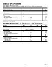
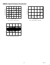
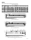
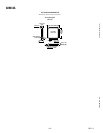
The CDS stage has a default gain of 4 dB, but uses a unique
architecture that allows the CDS gain to be varied. Using the
CDS Gain Register, the gain-of is programmable from –2 dB to
+10 dB in 64 steps, using two’s complement coding. The CDS
Gain curve is shown in Figure 12. To change the gain of the
CDS using the CDS Gain Register, the Control Register Bit D3
must be set high (CDS Gain Enabled). The default gain setting
when bit Control Register bit D3 is low (CDS Gain Disabled) is
4 dB. See Tables V and VI for more details.
A CDS gain of 4 dB provides some front-end signal gain and
improves the overall signal-to-noise ratio. This gain setting
works very well in most applications, and the CCD-Mode
Specifications use this default gain setting. However, the CDS
gain may be varied to optimize the AD9843A operation in a
particular application. Increased CDS gain can be useful with
low output level CCDs, while decreased CDS gain allows the
AD9843A to accept CCD signal swings greater than 1 V p-p.
Table VII summarizes some example CDS gain settings for
different maximum signal swings. The CDS Gain Register may
also be used “on the fly” to provide a +6 dB boost or –6 dB
attenuation when setting exposure levels. It is best to keep the
CDS output level from exceeding 1.5 V~1.6 V.
Table VII. Example CDS Gain Settings
Recommended
Max Input Signal Gain Range Register Code Range
250 mV p-p 8 to 10 dB 21 to 31
500 mV p-p 6 to 8 dB 10 to 21
800 mV p-p 4 to 6 dB 63 to 10
1 V p-p 2 to 4 dB 53 to 63
1.25 V p-p 0 to 2 dB
42 to 53
1.5 V p-p –2 to 0 dB 32 to 42
CDS GAIN REGISTER CODE
10
32
CDS GAIN – dB
40 48 56 0 8 16 24 31
8
6
4
2
0
-2
(100000)
(011111)
Figure 12. CDS Gain Curve
Input Clamp
A line-rate input clamping circuit is used to remove the CCD’s
optical black offset. This offset exists in the CCD’s shielded
black reference pixels. Unlike some AFE architectures, the
AD9843A removes this offset in the input stage to minimize the
effect of a gain change on the system black level, usually called
the “gain step.” Another advantage of removing this offset at the
input stage is to maximize system headroom. Some area CCDs
have large black level offset voltages, which, if not corrected at
the input stage, can significantly reduce the available headroom
in the internal circuitry when higher VGA gain settings are used.
Horizontal timing is shown in Figure 6. It is recommended
that the CLPDM pulse be used during valid CCD dark pixels.
CLPDM may be used during the optical black pixels, either