


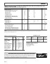

AD9843A
–15–
REV. 0
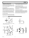
APPLICATIONS INFORMATION
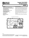
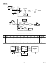
The AD9843A is a complete Analog Front End (AFE) product
for digital still camera and camcorder applications. As shown in
Figure 16, the CCD image (pixel) data is buffered and sent to
the AD9843A analog input through a series input capacitor.
The AD9843A performs the dc restoration, CDS, gain adjust-
ment, black level correction, and analog-to-digital conversion.
The AD9843A’s digital output data is then processed by the
image processing ASIC. The internal registers of the AD9843A
—used to control gain, offset level, and other functions—are
programmed by the ASIC or microprocessor through a 3-wire
serial digital interface. A system timing generator provides the
clock signals for both the CCD and the AFE.
Internal Power-On Reset Circuitry
After power-on, the AD9843A will automatically reset all inter-
nal registers and perform internal calibration procedures. This
takes approximately 1 ms to complete. During this time, normal
clock signals and serial write operations may occur. However,
serial register writes will be ignored until the internal reset
operation is completed. Pin 43 (formerly RSTB on the AD9843
non-A) is no longer used for the reset operation. Toggling Pin
43 in the AD9843A will have no effect.
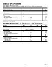
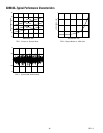
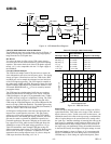
Grounding and Decoupling Recommendations
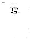
As shown in Figure 17, a single ground plane is recommended
for the AD9843A. This ground plane should be as continu-
ous as possible, particularly around Pins 25 through 39. This
will ensure that all analog decoupling capacitors provide the lowest
possible impedance path between the power and bypass pins
and their respective ground pins. All decoupling capacitors
should be located as close as possible to the package pins. A
single clean power supply is recommended for the AD9843A,
but a separate digital driver supply may be used for DRVDD
(Pin 13). DRVDD should always be decoupled to DRVSS (Pin
14), which should be connected to the analog ground plane.
Advantages of using a separate digital driver supply include
using a lower voltage (2.7 V) to match levels with a 2.7 V ASIC,
reducing digital power dissipation, and reducing potential noise
coupling. If the digital outputs (Pins 3–12) must drive a load
larger than 20 pF, buffering is recommended to reduce digital
code transition noise. Alternatively, placing series resistors
close to the digital output pins may help reduce noise.
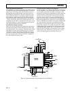
DRVDD
DRVSS
DVSS
DATACLK
DVDD1
DVSS
PBLK
CLPOB
SHP
SHD
CLPDM
DVSS
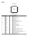
13 14 15 16 17 18 19 20 21 22 23 24
1
2
3
4
5
6
7
8
9
10
11
12
3748 47 46 45 44 39 3843 42 41 40
PIN 1
IDENTIFIER
TOP VIEW
(Not to Scale)
AD9843A
36
35
34
33
32
31
30
29
28
27
26
25
AUX1IN
AVSS
AUX2IN
AVDD2
BYP4
NC
CCDIN
BYP2
BYP1
AVDD1
AVSS
AVSS
DRVSS
DRVSS
(LSB) D0
D1
D2
D3
D4
D5
D6
D7
D8
(MSB) D9
SCK
SDATA
SL
NC
STBY
NC
THREE-STATE
DVSS
DVDD2
VRB
VRT
CML
0.1F
0.1F
0.1F
0.1F
0.1F
0.1F
3V
ANALOG
SUPPLY
CCD
SIGNAL
3V
ANALOG
SUPPLY
10
DATA
OUTPUTS
3
SERIAL
INTERFACE
0.1F
1.0F
1.0F
0.1F
3V
ANALOG SUPPLY
6
CLOCK
INPUTS
0.1F
0.1F
3V
ANALOG SUPPLY
3V
DRIVER
SUPPLY
NC = NO CONNECT
Figure 17. Recommended Circuit Configuration for CCD-Mode