


–3–
REV. 0
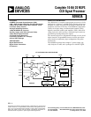
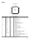
AD9843A
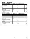
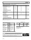
Parameter Min Typ Max Unit Notes
P
OWER CONSUMPTION 78 mW See TPC 1 for Power Curves
MAXIMUM CLOCK RATE 20 MHz
CDS
Allowable CCD Reset Transient
1
500 mV See Input Waveform in Note 1
Max CCD Black Pixel Amplitude
1
200 mV
Max Input Range Before Saturation
1
1.0 V p-p With 4 dB CDS Gain
Max Input Range Before Saturation 1.5 V p-p With –2 dB CDS Gain
Max Input Range Before Saturation 0.5 V p-p With 10 dB CDS Gain
Max Output Range 1.6 V p-p At Any CDS Gain Setting
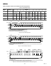
Gain Resolution 64 Steps
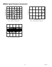
Gain Range (Two’s Complement Coding) See Figure 12 for CDS Gain Curve
Min Gain (CDS Gain Register Code 32) –2 dB
Medium Gain (CDS Gain Code 63) 4 dB 4 dB Is Default with CDS Gain Disabled
Max Gain (CDS Gain Code 31) 10 dB
VARIABLE GAIN AMPLIFIER (VGA)
Max Input Range 1.6 V p-p
Max Output Range 2.0 V p-p
Gain Control Resolution 1024 Steps
Gain Monotonicity Guaranteed
Gain Range See Figure 13 for VGA
Gain Curve
Low Gain (VGA Register Code 91) 2 dB See Page 13 for Gain Equations
Max Gain (VGA Code 1023) 36 dB
BLACK LEVEL CLAMP
Clamp Level Resolution 256 Steps
Clamp Level Measured at ADC Output
Min Clamp Level 0 LSB
Max Clamp Level 63.75 LSB
SYSTEM PERFORMANCE Specifications Include Entire Signal Chain
Gain Accuracy, VGA Code 91 to 1023 –0.5 +0.5 dB Use Equations on Page 13 to Calculate Gain
Peak Nonlinearity, 500 mV Input Signal 0.1 % 12 dB Gain Applied (4 dB CDS Gain)
Peak Nonlinearity, 800 mV Input Signal 0.4 % 8 dB Gain Applied (4 dB CDS Gain)
Total Output Noise 0.2 LSB rms AC Grounded Input, 6 dB Gain Applied
Power Supply Rejection (PSR) 40 dB Measured with Step Change on Supply
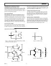
POWER-UP RECOVERY TIME Clocks Must Be Applied, as in Figures 5 and 6
From Fast Recovery Mode 0.1 ms
From Reference Standby Mode 1 ms
From Total Shutdown Mode 3 ms
From Power-Off Condition 15 ms
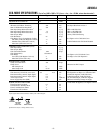
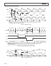
NOTES
1
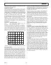
Input Signal Characteristics defined as follows, with 4 dB CDS gain:
1V MAX
INPUT
SIGNAL RANGE
200mV MAX
OPTICAL
BLACK PIXEL
500mV TYP
RESET
TRANSIENT
Specifications subject to change without notice.
CCD-MODE SPECIFICATIONS
(T
MIN
to T
MAX
, AVDD = DVDD = 3.0 V, f
DATACLK
= f
SHP
= f
SHD
= 20 MHz, unless otherwise noted.)