


swru266
19/25
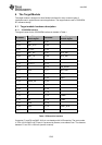
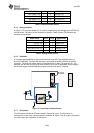
UART CTS(P1.3) 5 6 UART RTS(P2.18)
SPI CSN(P1.14) 7 8 SCLK(P1.16)
MOSI(P1.18) 9 10 MISO(P1.20)
I2C SDA(P1.11) 11 12 I2C SCL(P1.5)
EM_RESET((P2.15) 13 14 IR_OUT1(P1.13)
Table 2: Interface header pinout
6.1.5 Debug interface
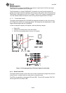
A 2x5 pin 1.27 mm pitch header (J5) is used for programming and debugging the CC2533 on
the EM socket. The pinout of this connector is shown in Table 3 below. EM connector pin
numbers in parentheses.
Signal name Pin # Pin # Signal name
GND 1 2 VDD
DC(P1.12) 3 4 DD(P1.10)
CSN(P1.14) 5 6 SCLK(P1.16)
EM_RESET(P2.15) 7 8 MOSI(P1.18)
NC 9 10 MISO(P1.20)
Table 3: Debug Header pinout
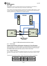
6.1.6 Dataflash
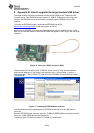
A 2 megabit serial dataflash on the board interfaces to the SPI. The dataflash used is a
Numonyx M25PE20. The flash SPI interface is connected to the SPI interface on the EM
connector. The flash chip select signal is controlled by the FLASH_CS signal (P1.4). The
dataflash can be used for storing IR code libraries or Over the Air Download (OAD) images if
the devices support downloading new program memory from the RF interface.
Figure 12: Serial flash interface details
6.1.7 IR Interface
The IR interface includes an IR receiver and 1 channel IR output. The IR receiver is
connected to a timer input capture channel to measure IR signals. The IR output is connected
to a timer output pin to generate IR waveforms.