


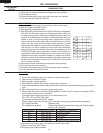
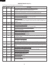
20
MMD24S
MMD24B
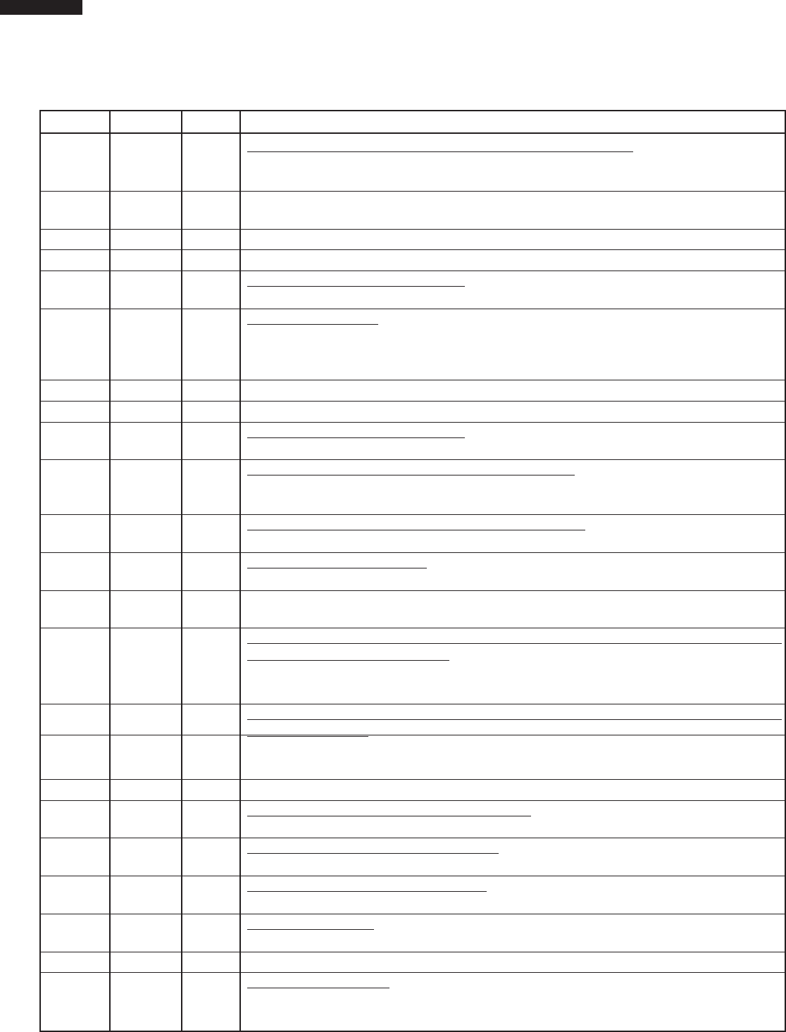
1 - 3 AN5- AN3 IN Terminal to change cooking input according to the Model.
By using A/D converter contained in the LSI, DC voltage in accordance with the Model
in operation is applied to set up its cooking constant.
4 AN2 IN Input signal which inform the drawer door is in the middle position between the opened
position and the closed position, to LSI from the door position switch rear.
5 AN1 IN Terminal not used.
6 AN0 IN Terminal not used.
7 CNVSS IN Power source voltage: 0V (GND).
VC voltage of power source circuit input. Connected GND.
8 RESET IN Auto clear terminal.
Signal is input to reset the LSI to the initial state when power is applied. Temporarily set
to “L” level the moment power is applied, at this time the LSI is reset. Thereafter set at
“H” level.
9 P62 OUT Terminal not used.
10 P61 IN/OUT Terminal not used.
11 VSS IN Power source voltage: 0V (GND).
VS voltage of power source circuit input. Connected GND.
12 XIN IN Internal clock oscillation frequency setting input.
The internal clock frequency is set by inserting the ceramic filter oscillation circuit with
respect to Xout terminal.
13 XOUT OUT Internal clock oscillation frequency control output.
Output to control oscillation input of Xin.
14 VCC IN Power source voltage: +5V.
VC voltage of power source circuit input.
15 P60 IN Plus signal coming from the Microwave drawer door open-close motor is input into P60
as revolution number.
16 P37 IN Input signal which communicates the drawer door open information to LSI from
the door position switch front.
Door opened; “L” level signal(0V).
Door closed; “H” level signal(+5V).
17 P36 OUT Signal to change the rotational direction is output to the Microwave drawer door
open-close motor.
18 TXOUT OUT Signal to change the rotational speed is output to the Microwave drawer door open-close
motor.
19 P34 OUT Power source to drive the Microwave drawer door open-close motor is output.
20 RXD2 IN Input terminal to check the data of display.
Data signal from IC-2 is input to RXD2 to check the flow of the data.
21 TXD2 IN Output terminal to send IC-2 the data.
The data of display is output to IC-2.
22 SCLK2 OUT Clock timing signaI output terminal.
Clock timing signal is sent to IC-2.
23 P30 OUT Signal to reset LSI.
Signal is output to reset IC-2.
24 - 25
COM3 - COM2
OUT Terminal not used.
26 COM1 OUT Common data signal.
Connected to LCD signal C5.
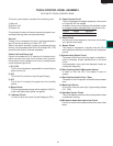
DESCRIPTION OF LSI (IC-1)
The I/O signal of the LSIis detailed in the following table.
Pin No. Signal I/O Description