


www.amctechcorp.com 15
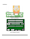
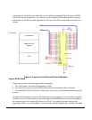
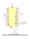
The CPU Architecture consists of 4 main functional regions. The Ethernet Controller, the PCI
Interface, the MCU Core and System Memory. These regions form a highly integrated embedded
system. The Backplane Architecture consists of 3 main regions. The Communication Connec-
tors, the DIMM and PCI Slots and the LCD Connector. These regions complete the dimmPCI
TM
system.
The MCU Core
The MC68VZ328 provides system designers more performance with the capability of running at
higher speed while achieving lower power consumption with a true static core. The MCU
features a fully static synthesizable FLX68000 Core Processor. This processor provides more
than 5 MIPS performance at 33MHz processor clock. The DragonBall VZ also provides a UART,
Timer/PWM, Parallel I/O, LCD Controller, DRAM/SDRAM Controller, SPI, and RTC.
System Memory
The module provides up to 8 MB of FLASH ROM and up to 32 MB of SDRAM. These are
configured as 16-bit wide memories. The SDRAM controller has been configured to use self
refresh and also supports CAS-before-RAS refresh cycles. Low power mode control also comes
into effect on the MC68VZ328.
The LCD utilizes the main system memory as the display memory. With SDRAM there is a single
LCD DMA cycle transfer.
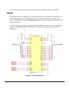
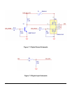
Memory Map
The Dragonball VZ has four pairs of chip selects, CSA0 & CSA1, CSB0 & CSB1, CSC0 & CSC1,
and CSD0 & CSD1. Individual chip selects are not completely configurable; rather, the chip
selects are configured as pairs. Chip select pairs share a base address (the addressable region of
the second chip select begins immediately after the addressable region of the first), the size of
the addressable area (relative to the base address), the number of wait states, and whether it is
an 8-bit or a 16-bit chip select.
When SDRAM is enabled, the Dragonball VZ consumes five of the chip selects. CSB1, CSC0,
CSC1 become WE, RAS, CAS and CSD0, CSD1 become CS suitable for SDRAM only. The 16-bit
flash has been assigned to CSA0, because that is the only chip select active after reset. The wait
states are set for internal timing.
The 16-bit CY7C09449 PCI interface is a synchronous interface and must be attached to CSB0,
which is configured for external timing (“infinite” wait states).