


AD8342
Rev. 0 | Page 16 of 20
IF PORT
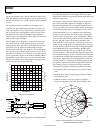
The IF port comprises open-collector differential outputs. The
NPN open collectors can be modeled as current sources that are
shunted with resistances of ~10 kΩ in parallel with capacitances
of ~1 pF.
The specified performance numbers for the AD8342 were
measured with 100 Ω differential terminations. However, dif-
ferent load impedances may be used where circumstances dic-
tate. In general, lower load impedances result in lower conver-
sion gain and lower output P1dB. Higher load impedances
result in higher conversion gain for small signals, but lower IP3
values for both input and output.
If the IF signal is to be delivered to a remote load, more than a
few millimeters away at high output frequencies, avoid unin-
tended parasitic effects due to the intervening PCB traces. One
approach is to use an impedance transforming network or
transformer located close to the AD8342. If very wideband out-
put is desired, a nearby buffer amplifier may be a better choice,
especially if IF response to dc is required. An example of such a
circuit is presented in Figure 45, in which the AD8351 differen-
tial amplifier is used to drive a pair of 75 Ω transmission lines.
The gain of the buffer can be independently set by appropriate
choice of the value for the gain resistor, R
G
.
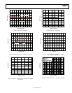
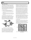
50
0.5
0
0
1G
05352-045
FREQUENCY (Hz)
RESISTANCE (kΩ)
CAPACITANCE (pF)
45
0.4
40
0.3
35
0.2
30
0.1
25
0
20
–0.1
15
–0.2
10
5
100M 200M 300M 400M 500M 600M 700M 800M 900M
Figure 44. IF Port Impedance
05352-046
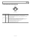
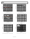
COMM
8
IFOP
7
IFOM
6
COMM
5
AD8342
AD8351
+
–
R
F
C
+
V
S
R
F
C
Z
L
=
1
0
0
Ω
+
V
S
+
V
S
100Ω R
G
Z
L
Tx LINE Z
O
= 75Ω
Tx LINE Z
O
= 75Ω
Figure 45. AD8351 Used as Transmission Line Driver and Impedance Buffer
The high input impedance of the AD8351 allows for a shunt
differential termination to provide the desired 100 Ω load to the
AD8342 IF output port.
It is necessary to bias the open-collector outputs using one of
the schemes presented in Figure 47 and Figure 48. Figure 47
illustrates the application of a center tapped impedance trans-
former. The turns ratio of the transformer should be selected to
provide the desired impedance transformation. In the case of a
50 Ω load impedance, a 2-to-1 impedance ratio transformer
should be used to transform the 50 Ω load into a 100 Ω differ-
ential load at the IF output pins. Figure 48 illustrates a differen-
tial IF interface where pull-up choke inductors are used to bias
the open-collector outputs. The shunting impedance of the
choke inductors used to couple dc current into the mixer core
should be large enough at the IF operating frequency so it does
not load down the output current before reaching the intended
load. Additionally, the dc current handling capability of the
selected choke inductors needs to be at least 45 mA. The self-
resonant frequency of the selected choke should be higher than
the intended IF frequency. A variety of suitable choke inductors
are commercially available from manufacturers such as Murata
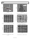
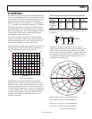
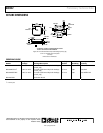
and Coilcraft. Figure 46 shows the loading effects when using
nonideal inductors. An impedance transforming network may
be required to transform the final load impedance to 100 Ω at
the IF outputs. There are several good reference books that
explain general impedance matching procedures, including:
• Chris Bowick, RF Circuit Design, Newnes, Reprint Edition,
1997.
• David M. Pozar, Microwave Engineering, Wiley Text Books,
Second Edition, 1997.
• Guillermo Gonzalez, Microwave Transistor Amplifiers:
Analysis and Design, Prentice Hall, Second Edition, 1996.
05352-049
0180
30
330
50MHz
50MHz
500MHz
500MHz
60
90
270
300
120
240
150
210
REAL
CHOKES
IDEAL
CHOKES
Figure 46. IF Port Loading Effects Due to Finite Q Pull-Up Inductors
(Murata BLM18HD601SN1D Chokes)