


AD8342
Rev. 0 | Page 17 of 20
05352-047
COMM
8
IFOP
7
IFOM
6
COMM
5
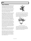
AD8342
Z
L
=
1
0
0
Ω
I
F
O
U
T
Z
O
=
5
0
Ω
+
V
S
2:1
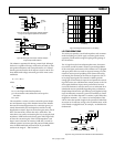
Figure 47. Biasing the IF Port Open-Collector Outputs
Using a Center-Tapped Impedance Transformer
05352-048
COMM
8
IFOP
7
IFOM
6
COMM
5
AD8342
R
F
C
+
V
S
R
F
C
Z
L
=
1
0
0
Ω
I
F
O
U
T
+
I
F
O
U
T
–
+
V
S
Z
L
IMPEDANCE
TRANSFORMING
NETWORK
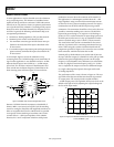
Figure 48. Biasing the IF Port Open-Collector Outputs
Using Pull-Up Choke Inductors
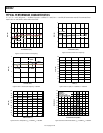
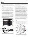
The AD8342 is optimized for driving a 100 Ω load. Although
the device is capable of driving a wide variety of loads, to main-
tain optimum distortion and noise performance, it is advised
that the presented load at the IF outputs is close to 100 Ω. The
linear differential voltage conversion gain of the mixer can be
modeled as
LOADm
RGAv ×=
where:
em
m
m
Rg
g
G
+
=
1
1
π
R
LOAD
is the single-ended load impedance.
g
m
is the transistor transconductance and is equal to
1810/R
BIAS
.
R
e
is 15 Ω.
The external R
BIAS
resistor is used to control the power dissipa-
tion and dynamic range of the AD8342. Because the AD8342
has internal resistive degeneration, the conversion gain is pri-
marily determined by the load impedance and the on-chip
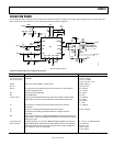
degeneration resistors. Figure 49 shows how gain varies with IF
load. The external R
BIAS
resistor has only a small effect. The
most direct way to affect conversion gain is by varying the load
impedance. Small loads result in lower gains while larger loads
increase the conversion gain. If the IF load impedance is too
large it causes a decrease in linearity (P1dB, IP3). In order to
maintain positive conversion gain and preserve SFDR perform-
ance, the differential load presented at the IF port should
remain in the range of ~ 100 Ω to 250 Ω.
30
0
10 1000
05352-057
IF LOAD (Ω)
VOLTAGE GAIN (dB)
100
25
20
15
10
5
MEASURED
MODELED
Figure 49. Voltage Conversion Gain vs. IF Loading
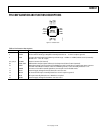
LO CONSIDERATIONS
The LOIN port provides a 50 Ω load impedance with common-
mode decoupling on LOCM. Again, common-grade ceramic
capacitors provide sufficient signal coupling and bypassing of
the LO interface.
The LO signal needs to have adequate phase noise characteris-
tics and low second-harmonic content to prevent degradation
of the noise figure performance of the AD8342. An LO plagued
with poor phase noise can result in reciprocal mixing, a mecha-
nism that causes spectral spreading of the downconverted sig-
nal, limiting the sensitivity of the mixer at frequencies close-in
to any large input signals. The internal LO buffer provides
enough gain to hard-limit the input LO and provide fast switch-
ing of the mixer core. Odd harmonic content present on the LO
drive signal should not impact mixer performance; however,
even-order harmonics cause the mixer core to commutate in an
unbalanced manner, potentially degrading noise performance.
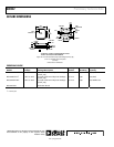
Simple lumped element low-pass filtering can be applied to help
reject the harmonic content of a given local oscillator, as shown
in Figure 50. The filter depicted is a common 3-pole Chebyshev,
designed to maintain a 1-to-1 source-to-load impedance ratio
with no more than 0.5 dB of ripple in the pass band. Other filter
structures can be effective as long as the second harmonic of the
LO is filtered to negligible levels, for example, ~30 dB below the
fundamental.
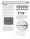
05352-050
AD8342
LOIN
3
COMM
4
LOCM
2
R
L
FOR R
S
= R
L
f
C
- FILTER CUTOFF FREQUENCY
R
S
C1 C3
LO
SOURCE
L2
C1 =
1.864
2
πf
c
R
L
C3 =
1.834
2
πf
c
R
L
L2 =
1.28R
L
2πf
c
Figure 50. Using a Low-Pass Filter to Reduce LO Second Harmonic