


AD8342
Rev. 0 | Page 7 of 20
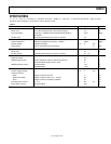
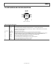
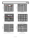
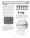
PIN CONFIGURATION AND FUNCTION DESCRIPTIONS
05352-002
PIN 1
INDICATOR
1VPLO
2LOCM
3LOIN
4COMM
11 PWDN
12 VPDC
10 EXRB
9 COMM
5
C
O
M
M
6
I
F
O
M
7
I
F
O
P
8
C
O
M
M
1
5
R
F
I
N
1
6
V
P
M
X
1
4
R
F
C
M
1
3
C
O
M
M
TOP VIEW
(Not to Scale)
AD8342
Figure 2. 16-Lead LFCSP
Table 5. Pin Function Descriptions
Pin No. Mnemonic Function
1 VPLO Positive Supply Voltage for the LO Buffer: 4.75 V to 5.25 V.
2 LOCM
AC Ground for Limiting LO Amplifier. Internally biased to Vs − 1.6 V. AC-couple to ground.
3 LOIN
LO Input. Nominal input level 0 dBm. Input level range −10 dBm to +4 dBm (relative to 50 Ω). Internally
biased to Vs − 1.6 V. AC-couple.
4, 5, 8, 9, 13 COMM Device Common (DC Ground).
6, 7 IFOM, IFOP Differential IF Outputs (Open Collectors). Each requires dc bias of 5.00 V (nominal).
10 EXRB
Mixer Bias Voltage. Connect resistor from EXRB to ground. Typical value of 1.82 kΩ sets mixer current to
nominal value. Minimum resistor value from EXRB to ground = 1.8 kΩ. Internally biased to 1.17 V.
11 PWDN Connect to Ground for Normal Operation. Connect pin to V
S
for disable mode.
12 VPDC Positive Supply Voltage for the DC Bias Cell: 4.75 V to 5.25 V.
14 RFCM AC Ground for RF Input. Internally biased to 2.4 V. AC-couple to ground.
15 RFIN RF Input. Internally biased to 2.4 V. Must be ac-coupled.
16 VPMX Positive Supply Voltage for the Mixer: 4.75 V to 5.25 V.