


AD8342
Rev. 0 | Page 18 of 20
HIGH IF APPLICATIONS
In some applications it may be desirable to use the AD8342 as
an up-converting mixer. The AD8342 is a broadband mixer
capable of both up and down conversion. Unlike other mixers
that rely on on-chip reactive circuitry to optimize performance
over a specific band, the AD8342 is a versatile general-purpose
device that can be used from arbitrarily low frequencies to sev-
eral GHz. In general, the following considerations help to en-
sure optimum performance:
• Minimize ac loading impedance of IF port bias network.
• Maximize power transfer to the desired ac load.
• For maximum conversion gain and the lowest noise per-
formance reactively match the input as described in the
IF Port section.
• For maximum input compression point and input intercept
points resistively terminate the input as described in the
IF Port section.
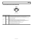
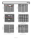
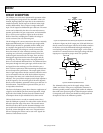
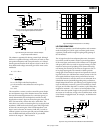
As an example, Figure 51 shows the AD8342 as an up-
converting mixer for a WCDMA single-carrier transmitter de-
sign. For this application, it was desirable to achieve −65 dBc
adjacent channel power ratio (ACPR) at a −13 dBm output
power level. The ACPR is a measure of both distortion and
noise carried into an adjacent frequency channel due to the
finite intercept points and noise figure of an active device.
8
7
6
13
15
16
COMM
IFOP
IFOM
5
COMM
14
2
1
3
4
COMM
RFCM
RFIN
VPMX
VPDC PWDN EXRB COMM
1
1
1
2
1
0
9
VPLO LOCM LOIN COMM
AD8342
05352-052
VPOS
VPOS
34nH
34nH
100pF
100pF
1nF
1nF
ETC1-1-13
100pF
100pF0.1µF
VPOS
1nF
1nF
1970MHz
OSC
1.82kΩ
100pF
4.7pF
170MHz
INPUT
100nH
1nF
499Ω
VPOS
100pF0.1pF
2140MHz OUT
1nF
Figure 51. WCDMA Tx Up-Conversion Application Circuit
Because a WCDMA channel encompasses a bandwidth of
almost 5 MHz, it is necessary to keep the Q of the matching
circuit low enough so that phase and magnitude variations are
below an acceptable level over the 5 MHz band. It is possible
to use purely reactive matching to transform a 50 Ω source
to match the raw ~1 kΩ input impedance of the AD8342.
However, the L and C component variations could present
production concerns due to the sensitivity of the match. For
this application, it is advantageous to shunt down the ~1 kΩ
input impedance using an external shunt termination resistor
to allow for a lower Q reactive matching network. The input is
terminated across the RFIN and RFCM pins using a 499 Ω
termination. The termination should be as close to the device as
possible to minimize standing wave concerns. The RFCM is
bypassed to ground using a 1 nF capacitor. A dc blocking ca-
pacitor of 1 nF is used to isolate the dc input voltage present on
the RFIN pin from the source. A step-up impedance transfor-
mation is realized using a series L shunt C reactive network.
The actual values used need to accommodate for the series L
and stray C parasitics of the connecting transmission line seg-
ments. When using the customer evaluation board with the
components specified in Figure 51, the return loss over a 5 MHz
band centered at 170 MHz was better than 10 dB.
External pull-up choke inductors are used to feed dc bias into
the open-collector outputs. It is desirable to select pull-up choke
inductors that present high loading reactance at the output
frequency. Coilcraft 0302CS series inductors were selected due
to their very high self-resonant frequency and Q. A 1:1 balun
was ac-coupled to the output to convert the differential output
to a single-ended signal and present the output with a 50 Ω
ac loading impedance.
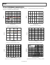
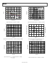
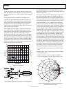
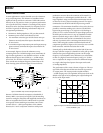
The performance of the circuit is shown in Figure 52. The aver-
age ACPR of the adjacent and alternate channels is presented
vs. output power. The circuit provides a 65 dBc ACPR at
−13 dBm output power. The optimum ACPR power level can be
shifted to the right or left by adjusting the output loading and
the loss of the input match.
–60
–70
–25 0
05352-053
OUTPUT POWER (dBm)
ACPR (dBc)
–62
–64
–66
–68
–20 –15 –10 –5
ADJACENT
CHANNELS
ALTERNATE
CHANNELS
Figure 52. Single Carrier WCDMA ACPR Performance of Tx Up-Conversion
Circuit (Test Model 1_64)