


AD8342
Rev. 0 | Page 19 of 20
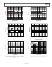
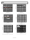
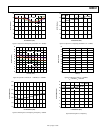
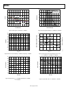
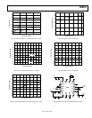
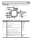
EVALUATION BOARD
An evaluation board is available for the AD8342. The evaluation board is configured for single-ended signaling at the IF output port via a
balun transformer. The schematic for the evaluation board is presented in Figure 53.
R2
0Ω
R1
0Ω
C6
1000pF
C4
1000pF
C1
1000pF
C3
1000pF
C5
0.1µF
C2
0.1µF
VPOS
RF_IN
C7
1000pF
INLO
C8
1000pF
C9
0.1µF
C10
100pF
VPOS
R11
0Ω
R16
0Ω
R10
0Ω
R12
OPEN
Z4
OPEN
R4
OPEN
34
16
2
TC2-1T
Z2
OPEN
R3
OPEN
100Ω TRACES,
NO GROUND PLANE
IF_OUT+
IF_OUT–
R15
0Ω
T1
Z1
OPEN
Z3
OPEN
R5
100Ω
C14
OPEN
L1
0Ω
COMM
IFOP
IFOM
COMM
COMM
RFCM
RFIN
VPMX
VPDC
PWDN
EXRB
COMM
VPLO
LOCM LOIN
COMM
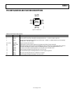
DUT
12
11
10
9
13
14
15
16
1
2
3
4
8
7
6
5
R6
1.82kΩ
C11
100pF
R7
0Ω
C13
100pF
C12
0.1µF
VPOSGND
PWDN
VPOS
W1
R8
10kΩ
R9
0Ω
PWDN
05352-003
50Ω
TRACE
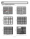
Figure 53. Evaluation Board
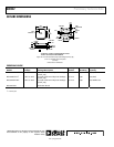
Table 6. Evaluation Board Configuration Options
Component Function Default Conditions
R1, R2, R7,
C2, C4, C5, C6, C10
C12, C13, C14, C9
Supply decoupling. Shorts or power supply decoupling resistors and filter
capacitors.
R1, R2, R7 = 0 Ω
C4, C6 = 1000 pF
C10, C13 = 100 pF
C2, C5, C12, C9 = 0.1 µF
R3, R4 Options for single-ended IF output circuit. R3, R4 = Open Ω
R15, 16 R15, R16 = 0 Ω
R6, C11
R
BIAS
resistor that sets the bias current for the mixer core. The capacitor
provides ac bypass for R6.
R6 = 1.82 kΩ
C11 = 100 pF
R8 Pull down for the PWDN pin. R8 = 10 kΩ
R9 Link to PWDN pin. R9 = 0 Ω
C3, R5, C16, L1
RF input. C3 provides dc block for RF input. R5 provides a resistive input
termination. C16 and L1 are provided for reactive matching the input.
C3 = 1000 pF
R5 = 100 Ω
C14 = Open
L1 = 0 Ω
C1
RF common ac coupling. Provides dc block for RF input common
connection.
C1 = 1000 pF
C8
C7
LO input ac coupling. Provides dc block for the LO input.
LO common ac coupling. Provides dc block for LO input common
connection.
C7, C8 = 1000 pF
W1
Power down. The part is on when the PWDN is connected to ground via a
10 kΩ resistor. The part is disabled when PWDN is connected to the positive
supply (V
S
) via W1.
T1, R12, R11, Z3,
Z4, Z1, Z2, R10
IF output interface. T1 converts a differential high impedance IF output to
single-ended. When loaded with 50 Ω, this balun presents a 100 Ω load to
the mixers collectors. The center tap of the primary is used to supply the
bias voltage (V
S
) to the IF output pins.
T1 = TC2-1T, 2:1 (Mini-Circuits)
R12 = Open Ω
R10, R11 = 0 Ω
Z3, Z4 = Open
Z1, Z2 = Open