


AWARD
®
BIOS Setup
3-13
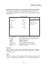
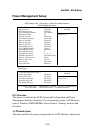
Note: Change these settings only if you are familiar with the chipset.
Configure SDRAM Timing
Selects whether DRAM timing is controlled by the SPD (Serial Presence
Detect) EEPROM on the DRAM module. Setting to By SPD enables CAS#
Latency, RAS# Precharge, RAS# to CAS# Delay and RAS# Precharge
automatically to be determined by BIOS based on the configurations on the
SPD. Selecting By Manual allows users to configure these fields manually.
CAS# Latency
This controls the timing delay (in clock cycles) before SDRAM starts a read
command after receiving it. Settings: 1.5, 2, 2.5 and 3 (clocks). 1.5 (clocks)
increases the system performance the most while 3 (clocks) provides the
most stable performance.
Precharge Delay
The field specifies the idle cycles before precharging an idle bank. Settings:
7, 6 and 5 (clocks).
Advanced Chipset Features
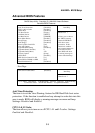
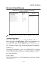
↑↓→←:Move Enter:Select +/-/PU/PD:Value F10:Save ESC:Exit F1:General Help
F5:Previous Values F6:Fail-Safe Defaults F7:Optimized Defaults
Configure DRAM Timing [By SPD]
CAS# Latency [1.5]
Precharge Delay [7]
RAS# to CAS# Delay [3]
RAS# Precharge [3]
DRAM Data Integrity Mode [Non-ECC]
Memory Hole At 15M-16M [Disabled]
Delayed Transaction [Enabled]
AGP Aperture Size (MB) [64]
CMOS Setup Utility - Copyright (C) 1984-2001 Award Software
Advanced Chipset Features
Item Help
Menu Level 8