


VXI Technology, Inc.
24 SM7100 Programming
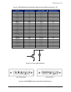
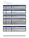
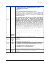
Offset Register (0x06) — Read and Write
D15-D0
A24/A32 Memory
Offset
The value written to this 16-bit register, times 256, sets the base
address of the A24 memory space used by the module. The value
written to this 16-bit register, times 65,536, sets the base address of
the A32 memory space used by the module. A read from this register
reflects the previously written value. Because of the required memory
size, bits D4 - D0 are disregarded on writes and always read back as 0.
Upon receiving a hard reset, all bits in this register are set to 0. A soft
reset does not affect the value in this register.
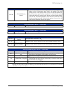
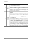
Reserved Register (0x0A) — Read Only
D15-D0 Not Implemented Always read back as FFFF
16
Reserved Register (0x0C) — Read Only
D15-D0 Not Implemented Always read back as FFFF
16
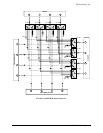
Version Number Register (0x0E) — Read Only
D15-D8
Firmware Version
Number
Not applicable, reads back as 00
16
D7-D4
Major Hardware
Version Number
Depends on the specific hardware revision of the SMIP II interface board.
D3-D0
Minor Hardware
Version Number
Depends on the specific hardware revision of the SMIP II interface board.
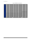
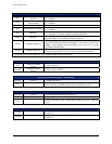
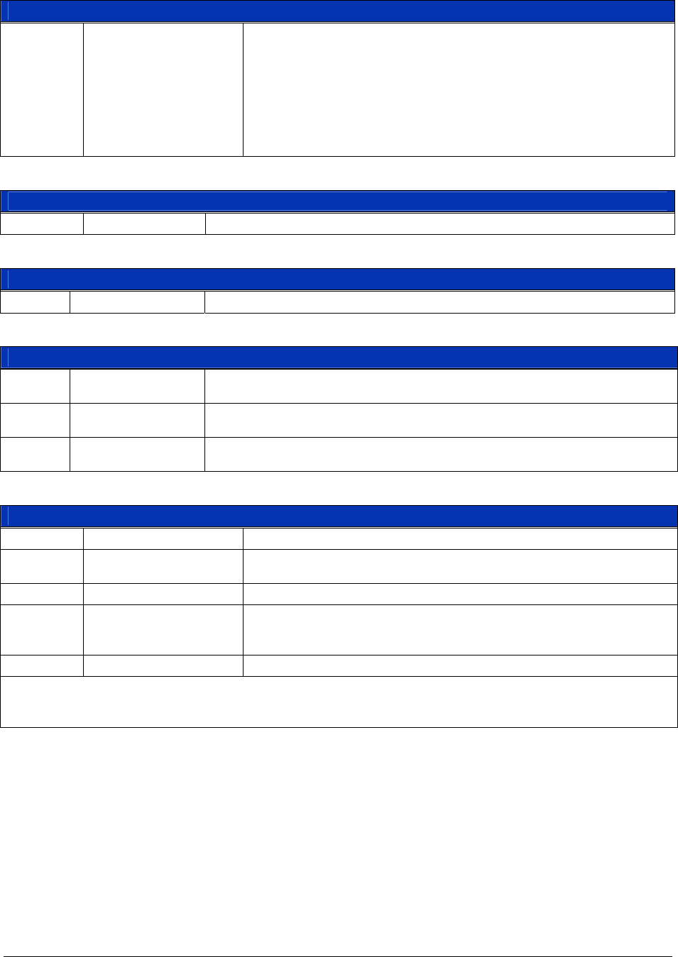
Interrupt Status Register (0x1A) — Read Only
D15 Scan Function done The latest scan list update is complete.
D14
Openbus Active Event
true
The Openbus was activated by one or more programmed inputs. See
description of the Openbus in the module register section.
D13-D9 Unused Data written to these bits have no effect.
D8 Module Busy Complete
The programmed Busy signal from the module has timed out. This
indicates that the relays actuated for that Busy cycle have settled and a
measurement may take place.
D7-D0 Reserved Always reads back as FFFF
16
Note: This status register may be used in a polled fashion rather than allowing the events above to generate an
Interrupt. A read of this register will clear any active bits. Bits that are not set, or are about to be set are not
affected by a read of this register.