


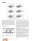
AD600/AD602
REV. A
–10–
1
2
3
4
5
6
7
8
16
15
14
13
12
11
10
9
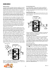
REF
A1
A2
C1HI
A1CM
A1OP
VPOS
VNEG
A2OP
A2CM
C2HI
C1LO
A1HI
A1LO
GAT1
GAT2
A2LO
A2HI
C2LO
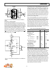
V '
G
C1
100pF
C4
0.1µF
R3
46.4kΩ
R4
3.74kΩ
R1
100Ω
AD600
+5V
DEC
–5V
DEC
RF
INPUT
AD590
R2
806Ω
1%
C3
15pF
300µA
(at 300K)
Q1
2N3904
V
PTAT
RF
OUTPUT
0.1µF
0.1µF
FB
–5V
+5V
POWER SUPPLY
DECOUPLING NETWORK
+5V DEC
–5V DEC
+5V
C2
1µF
+5V
FB
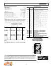
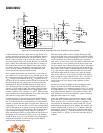
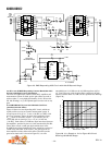
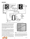
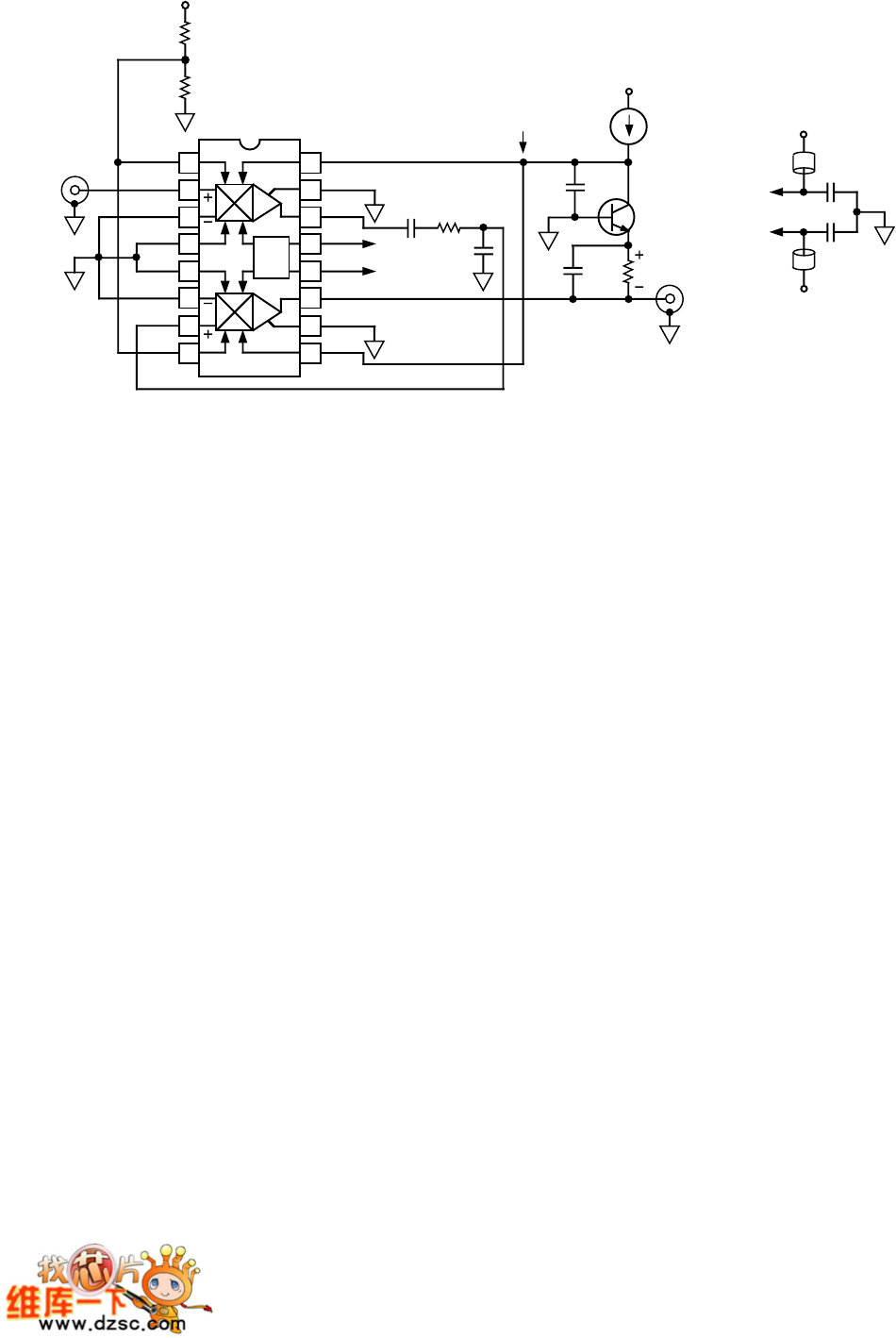
Figure 15. This Accurate HF AGC Amplifier Uses Just Three Active Components
A simple half-wave detector is used, based on Q1 and R2. The
average current into capacitor C2 is just the difference between
the current provided by the AD590 (300 µA at 300 K, 27°C)
and the collector current of Q1. In turn, the control voltage V
G
is the time integral of this error current. When V
G
(and thus the
gain) is stable, the rectified current in Q1 must, on average, ex-
actly balance the current in the AD590. If the output of A2 is
too small to do this, V
G
will ramp up, causing the gain to in-
crease, until Q1 conducts sufficiently. The operation of this
control system will now be described in detail.
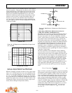
First, consider the particular case where R2 is zero and the out-
put voltage V
OUT
is a square wave at, say, 100 kHz, that is, well
above the corner frequency of the control loop. During the time
V
OUT
is negative, Q1 conducts; when V
OUT
is positive, it is cut
off. Since the average collector current is forced to be 300 µA, and
the square wave has a 50% duty-cycle, the current when con-
ducting must be 600 µA. With R2 omitted, the peak value of
V
OUT
would be just the V
BE
of Q1 at 600 µA (typically about
700 mV) or 2 V
BE
peak-to-peak. This voltage, hence the ampli-
tude at which the output stabilizes, has a strong negative tem-
perature coefficient (TC), typically –1.7 mV/°C. While this may
not be troublesome in some applications, the correct value of R2
will render the output stable with temperature.
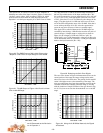
To understand this, first note that the current in the AD590 is
closely proportional to absolute temperature (PTAT). (In fact,
this IC is intended for use as a thermometer.) For the moment,
continue to assume that the signal is a square wave. When Q1 is
conducting, V
OUT
is the now the sum of V
BE
and a voltage which
is PTAT and which can be chosen to have an equal but opposite
TC to that of the base-to-emitter voltage. This is actually noth-
ing more than the “bandgap voltage reference” principle in
thinly veiled disguise! When we choose R2 such that the sum of
the voltage across it and the V
BE
of Q1 is close to the bandgap
voltage of about 1.2 V, V
OUT
will be stable over a wide range of
temperatures, provided, of course, that Q1 and the AD590
share the same thermal environment.
Since the average emitter current is 600 µA during each half-
cycle of the square wave, a resistor of 833 Ω would add a PTAT
voltage of 500 mV at 300 K, increasing by 1.66 mV/°C. In prac-
tice, the optimum value of R2 will depend on the transistor
used, and, to a lesser extent, on the waveform for which the tem-
perature stability is to be optimized; for the devices shown and
sine wave signals, the recommended value is 806 Ω. This resistor
also serves to lower the peak current in Q1 and the 200 Hz LP
filter it forms with C2 helps to minimize distortion due to ripple
in V
G.
Note that the output amplitude under sine wave condi-
tions will be higher than for a square wave, since the average
value of the current for an ideal rectifer would be 0.637 times as
large, causing the output amplitude to be 1.88 (= 1.2/0.637) V,
or 1.33 V rms. In practice, the somewhat nonideal rectifier
results in the sine wave output being regulated to about
1.275 V rms.
An offset of +375 mV is applied to the inverting gain-control
inputs C1LO and C2LO. Thus the nominal –625 mV to
+625 mV range for V
G
is translated upwards (at V
G
´) to –0.25 V
for minimum gain to +1 V for maximum gain. This prevents Q1
from going into heavy saturation at low gains and leaves suffi-
cient “headroom” of 4 V for the AD590 to operate correctly at
high gains when using a +5 V supply.
In fact, the 6 dB interstage attenuator means that the overall
gain of this AGC system actually runs from –6 dB to +74 dB.
Thus, an input of 2 V rms would be required to produce a 1 V
rms output at the minimum gain, which exceeds the 1 V rms
maximum input specification of the AD600. The available gain
range is therefore 0 dB to 74 dB (or, X1 to X5000). Since the
gain scaling is 15.625 mV/dB (because of the cascaded stages)
the minimum value of V
G
´ is actually increased by 6 × 15.625 mV,
or about 94 mV, to –156 mV, so the risk of saturation in Q1 is
reduced.