


AD600/AD602
REV. A
–3–
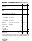
ABSOLUTE MAXIMUM RATINGS
1
Supply Voltage ±V
S
. . . . . . . . . . . . . . . . . . . . . . . . . . . . . . . . . . . . . . . . .
±7.5 V
Input Voltages
Pins 1, 8, 9, 16 . . . . . . . . . . . . . . . . . . . . . . . . . . . . . . . . ±V
S
Pins 2, 3, 6, 7 . . . . . . . . . . . . . . . . . . . . . . . ±2 V Continuous
. . . . . . . . . . . . . . . . . . . . . . . . . ±V
S
for 10 ms
Pins 4, 5 . . . . . . . . . . . . . . . . . . . . . . . . . . . . . . . . . . . . . ±V
S
Internal Power Dissipation
2
. . . . . . . . . . . . . . . . . . . .600 mW
Operating Temperature Range (J) . . . . . . . . . . . 0°C to +70°C
Operating Temperature Range (A) . . . . . . . . .–40°C to +85°C
Operating Temperature Range (S) . . . . . . . . .–55°C to +125°C
Storage Temperature Range . . . . . . . . . . . . .–65°C to +150°C
Lead Temperature Range (Soldering 60 sec) . . . . . . . . +300°C
NOTES
1
Stresses above those listed under “Absolute Maximum Ratings” may cause
permanent damage to the device. This is a stress rating only and functional
operation of the device at these or any other conditions above those indicated in the
operational section of this specification is not implied. Exposure to absolute
maximum rating conditions for extended periods may affect device reliability.
2
Thermal Characteristics: 16-Pin Plastic Package: θ
JA
= 85°C/Watt
16-Pin SOIC Package: θ
JA
= 100°C/Watt
16-Pin Cerdip Package: θ
JA
= 120°C/Watt
ORDERING GUIDE
Gain Temperatue Package
Model Range Range Option
1
AD600AQ 0 dB to +40 dB –40°C to +85°C Q-16
AD600AR 0 dB to +40 dB –40°C to +85°C R-16
AD602AQ –10 dB to +30 dB –40°C to +85°C Q-16
AD602AR –10 dB to +30 dB –40°C to +85°C R-16
AD600JN 0 dB to +40 dB 0°C to +70°C N-16
AD600JR 0 dB to +40 dB 0°C to +70°C R-16
AD602JN –10 dB to +30 dB 0°C to +70°C N-16
AD602JR –10 dB to +30 dB 0°C to +70°C R-16
AD600SQ/883B
2
0 dB to +40 dB –55°C to +150°C Q-16
AD602SQ/883B
3
–10 dB to +30 dB –55°C to +150°C Q-16
NOTES
1
N = Plastic DIP; Q= Cerdip; R= Small Outline IC (SOIC).
2
Refer to AD600/AD602 Military data sheet. Also available as 5962-9457201MPA.
3
Refer to AD600/AD602 Military data sheet. Also available as 5962-9457202MPA.
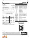
PIN DESCRIPTION
Pin Function Description
Pin 1 C1LO CH1 Gain-Control Input “LO” (Positive
Voltage Reduces CH1 Gain).
Pin 2 A1HI CH1 Signal Input “HI” (Positive Voltage
Increases CH1 Output).
Pin 3 A1LO CH1 Signal Input “LO” (Usually Taken to
CH1 Input Ground)
Pin 4 GAT1 CH1 Gating Input (A Logic “HI” Shuts Off
CH1 Signal Path).
Pin 5 GAT2 CH2 Gating Input (A Logic “HI” Shuts Off
CH2 Signal Path).
Pin 6 A2LO CH2 Signal Input “LO” (Usually Taken to
CH2 Input Ground).
Pin 7 A2HI CH2 Signal Input “HI” (Positive Voltage
Increases CH2 Output).
Pin 8 C2LO CH2 Gain-Control Input “LO” (Positive
Voltage Reduces CH2 Gain).
Pin 9 C2HI CH2 Gain-Control Input “HI” (Positive
Voltage Increases CH2 Gain).
Pin 10 A2CM CH2 Common (Usually Taken to CH2
Output Ground).
Pin 11 A2OP CH2 Output.
Pin 12 VNEG Negative Supply for Both Amplifiers.
Pin 13 VPOS Positive Supply for Both Amplifiers.
Pin 14 A1OP CH1 Output.
Pin 15 A1CM CH1 Common (Usually Taken to CH1
Output Ground).
Pin 16 C1HI CH1 Gain-Control Input “HI” (Positive
Voltage Increases CH1 Gain).
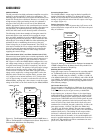
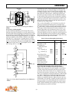
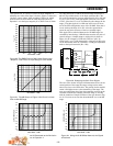
CONNECTION DIAGRAM
16-Pin Plastic DIP (N) Package
16-Pin Plastic SOIC (R) Package
16-Pin Cerdip (Q) Package
1
2
3
4
5
6
7
8
16
15
14
13
12
11
10
9
REF
A1
A2
C1HI
A1CM
A1OP
VPOS
VNEG
A2OP
A2CM
C2HI
C1LO
A1HI
A1LO
GAT1
GAT2
A2LO
A2HI
C2LO
AD600/AD602
CAUTION
ESD (electrostatic discharge) sensitive device. Permanent damage may occur on unconnected
devices subject to high energy electrostatic fields. Unused devices must be stored in conductive
foam or shunts. The protective foam should be discharged to the destination socket before
devices are removed.
WARNING!
ESD SENSITIVE DEVICE