


AD600/AD602
REV. A
–14–
100 dB to 120 dB RMS Responding Constant Bandwidth AGC
Systems with High Accuracy dB Outputs
The next two applications double as both AGC amplifiers and
measurement systems. In both, precise gain offsets are used to
achieve either (1) a very high gain linearity of ±0.1 dB over the
full 100 dB range, or (2) the optimal signal-to-noise ratio at any
gain.
A 100 dB RMS/AGC System with Minimal Gain Error
(Parallel Gain with Offset)
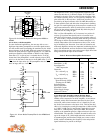
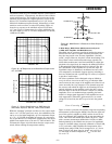
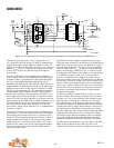
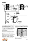
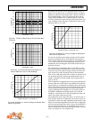
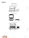
Figure 25 shows an rms-responding AGC circuit, which can
equally well be used as an accurate measurement system. It
accepts inputs of 10 µV to 1 V rms (–100 dBV to 0 dBV) with
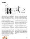
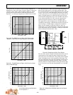
generous overrange. Figure 26 shows the logarithmic output,
V
LOG
, which is accurately scaled 1 V per decade, that is,
50 mV/dB, with an intercept (V
LOG
= 0) at 3.16 mV rms
(–50 dBV). Gain offsets of ±2 dB have been introduced between
the amplifiers, provided by the ±62.5 mV introduced by R6–R9.
These offsets cancel a small gain ripple which arises in the
X-AMP from its finite interpolation error, which has a period of
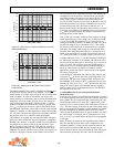
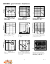
18 dB in the individual VCA sections. The gain ripple of all
three amplifier sections without this offset (in which case the
gain errors simply add) is shown in Figure 27; it is still a
remarkably low ±0.25 dB over the 108 dB range from 6 µV to
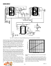
1.5 V rms. However, with the gain offsets connected, the gain
linearity remains under ±0.1 dB over the specified 100 dB range
(Figure 28).
5
3
–5
1µV10µV 10V1V100mV10mV1mV100µV
4
2
0
1
–1
–3
–2
–4
INPUT SIGNAL – V RMS
LOGARITHMIC OUTPUT – Volts
Figure 26. V
LOG
Plotted vs. V
IN
for Figure 25‘s Circuit
Showing 120 dB AGC Range
INPUT
1V RMS
MAX
(SINE WAVE)
1
2
3
4
5
6
7
8
16
15
14
13
12
11
10
9
REF
A1
A2
C1HI
A1CM
A1OP
VPOS
VNEG
A2OP
A2CM
C2HI
C1LO
A1HI
A1LO
GAT1
GAT2
A2LO
A2HI
C2LO
U1 AD600
+5V DEC
–5V DEC
U3A
1/4
AD713
R2
487Ω
V
OUT
C5
22µF
1
2
3
4
5
6
7
14
13
12
11
10
9
8
NC
NC
NC
–5V DEC
U3C
R11
46.4kΩ
+5V DEC
NC
NC
NC
1/4
AD713
+316.2mV
VINP
VNEG
CAVG
VLOG
BFOP
BFIN
VPOS
COMM
LDLO
V
U4
AD636
NC = NO CONNECT
C1
0.1µF
R3
200Ω
U3B
1/4
AD713
R1
133kΩ
C2
0.1µF
R5
1.58kΩ
R4
133kΩ
C3
220pF
1
2
3
4
5
6
7
8
16
15
14
13
12
11
10
9
REF
A1
A2
C1HI
A1CM
A1OP
VPOS
VNEG
A2OP
A2CM
C2HI
C1LO
A1HI
A1LO
GAT1
GAT2
A2LO
A2HI
C2LO
U2 AD600
+5V DEC
–5V DEC
C4
2µF
R6
10kΩ
+5V
–5V
R7
127Ω
R8
127Ω
R9
10kΩ
–2dB
–62.5mV
0dB
+2dB
+62.5mV
0.1µF
0.1µF
FB
–5V
+5V
POWER SUPPLY
DECOUPLING NETWORK
+5V DEC
–5V DEC
FB
R10
3.16kΩ
C6
4.7µF
V
LOG
Q1
2N3906
R14
301kΩ
R12
11.3kΩ
R13
3.01kΩ
R15
19.6kΩ
R16
6.65kΩ
+5V DEC
RMS
Figure 25. RMS Responding AGC Circuit with 100 dB Dynamic Range