


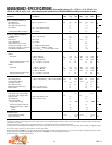

AD600J/AD602J AD600A/AD602A
Parameter Conditions Min Typ Max Min Typ Max Units
INPUT CHARACTERISTICS
Input Resistance Pins 2 to 3; Pins 6 to 7 98 100 102 95 100 105 Ω
Input Capacitance 22pF
Input Noise Spectral Density
1
1.4 1.4 nV/√Hz
Noise Figure R
S
= 50 Ω, Maximum Gain 5.3 5.3 dB
R
S
= 200 Ω, Maximum Gain 2 2 dB
Common-Mode Rejection Ratio f = 100 kHz 30 30 dB
OUTPUT CHARACTERISTICS
–3 dB Bandwidth V
OUT
= 100 mV rms 35 35 MHz
Slew Rate 275 275 V/µs
Peak Output
2
R
L
≥ 500 Ω±2.5 ±3 ±2.5 ±3V
Output Impedance f ≤ 10 MHz 2 2 Ω
Output Short-Circuit Current 50 50 mA
Group Delay Change vs. Gain f = 3 MHz; Full Gain Range ±2 ±2ns
Group Delay Change vs. Frequency V
G
= 0 V, f = 1 MHz to 10 MHz ±2 ±2ns
Total Harmonic Distortion R
L
= 200 Ω, V
OUT
= ±1 V Peak, Rpd = 1 kΩ –60 –60 dBc
ACCURACY
AD600
Gain Error 0 dB to 3 dB Gain 0 +0.5 +1 –0.5 +0.5 +0.5 dB
3 dB to 37 dB Gain –0.5 ±0.2 +0.5 –0.1 ±0.2 +1.0 dB
37 dB to 40 dB Gain –1 –0.5 0 –1.5 –0.5 +0.5 dB
Maximum Output Offset Voltage
3
V
G
= –625 mV to +625 mV 10 50 10 65 mV
Output Offset Variation V
G
= –625 mV to +625 mV 10 50 10 65 mV
AD602
Gain Error –10 dB to –7 dB Gain 0 +0.5 +1 –0.5 +0.5 +1.5 dB
–7 dB to 27 dB Gain –0.5 ±0.2 +0.5 –0.1 ±0.2 +1.0 dB
27 dB to 30 dB Gain –1 –0.5 0 –1.5 –0.5 +0.5 dB
Maximum Output Offset Voltage
3
V
G
= –625 mV to +625 mV 5 30 10 45 mV
Output Offset Variation V
G
= –625 mV to +625 mV 5 30 10 45 mV
GAIN CONTROL INTERFACE
Gain Scaling Factor 3 dB to 37 dB (AD600); –7 dB to 27 dB (AD602) 31.7 32 32.3 30.5 32 33.5 dB/V
Common-Mode Range –0.75 2.5 –0.75 2.5 V
Input Bias Current 0.35 1 0.35 1 µA
Input Offset Current 10 50 10 50 nA
Differential Input Resistance Pins I to 16; Pins 8 to 9 15 15 50 MΩ
Response Rate Full 40 dB Gain Change 40 40 dB/µs
SIGNAL GATING INTERFACE
Logic Input “LO” (Output ON) 0.8 0.8 V
Logic Input “HI” (Output OFF) 2.4 2.4 V
Response Time ON to OFF, OFF to ON 0.3 0.3 µs
Input Resistance Pins 4 to 3 Pins 5 to 6 30 30 kΩ
Output Gated OFF
Output Offset Voltage ±10 ؎100 ±10 ؎400 mV
Output Noise Spectral Density 65 65 nV/√Hz
Signal Feedthrough @ 1 MHz
AD600 –80 –80 dB
AD602 –70 –70 dB
POWER SUPPLY
Specified Operating Range ±4.75 ±5.25 ±4.75 ±5.25 V
Quiescent Current 11 12.5 11 14 mA
NOTES
1
Typical open or short-circuited input; noise is lower when system is set to maximum gain and input is short-circuited. This figure includes the effects of both voltage
and current noise sources.
2
Using resistive loads of 500 Ω or greater, or with the addition of a 1 kΩ pull-down resistor when driving lower loads
3
The dc gain of the main amplifier in the AD600 is X113; thus an input offset of only 100 µV becomes an 11.3 mV output offset. In the AD602, the amplifier’s gain is
X35.7; thus, an input offset of 100 µV becomes a 3.57 mV output offset.
Specifications shown in boldface are tested on all production units at final electrical test Results from those tests are used to calculate outgoing quality levels. All min
and max specifications guaranteed, although only those shown in boldface are tested on all production units.
Specifications subject to change without notice.
AD600/AD602–SPECIFICATIONS
(Each amplifier section, at T
A
= +25؇C, V
S
= ؎5 V, –625 mV ≤ V
G
≤
+625 mV, R
L
= 500 ⍀, and C
L
= 5 pF, unless otherwise noted. Specifications for AD600 and AD602 are identical unless otherwise noted.)
–2–
REV. A