


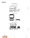
AD600/AD602
REV. A
–16–
1
2
3
4
5
6
7
8
16
15
14
13
12
11
10
9
REF
A1
A2
C1HI
A1CM
A1OP
VPOS
VNEG
A2OP
A2CM
C2HI
C1LO
A1HI
A1LO
GAT1
GAT2
A2LO
A2HI
C2LO
U1 AD600
+6V DEC
–6V DEC
U3A
1/4
AD713
R2
100Ω
V
OUT
C1
0.1µF
U3B
1/4
AD713
R1
133kΩ
C2
0.1µF
R5
5.36kΩ
R4
133kΩ
C3
0.001µF
1
2
3
4
5
6
7
8
16
15
14
13
12
11
10
9
REF
A1
A2
C1HI
A1CM
A1OP
VPOS
VNEG
A2OP
A2CM
C2HI
C1LO
A1HI
A1LO
GAT1
GAT2
A2LO
A2HI
C2LO
U2 AD600
+6V DEC
–6V DEC
C4
2µF
C5
22µF
1
2
3
4
5
6
7
14
13
12
11
10
9
8
NC
NC
NC
–6V DEC
U3C
R11
56.2kΩ
+6V DEC
NC
NC
NC
1/4
AD713
+316.2mV
VINP
VNEG
CAVG
VLOG
BFOP
BFIN
VPOS
COMM
LDLO
V
U4
AD636
NC = NO CONNECT
0.1µF
0.1µF
FB
–6V
+6V
POWER SUPPLY
DECOUPLING NETWORK
+6V DEC
–6V DEC
FB
R10
3.16kΩ
C6
4.7µF
V
LOG
R15
5.11kΩ
R14
7.32kΩ
+6V DEC
R13
866Ω
R12
1kΩ
INPUT
R17
115Ω
R3
200Ω
R6
3.4kΩ
+6V
R7
1kΩ
R8
294Ω
R9
1kΩ
R16
287Ω
0dB ADJUST
RMS
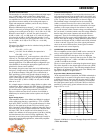
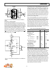
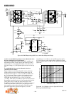
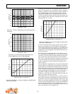
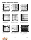
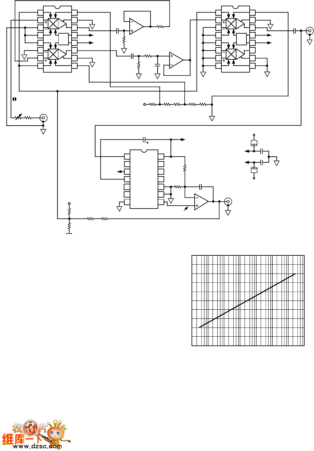
Figure 29. 120 dB Dynamic Range RMS Responding Circuit Optimized for S/N Ratio
resistance of U1A as well as the fixed 6 dB attenuation provided
by R2 and the input resistance of U1B are included both to set
V
LOG
to read 0 dB when V
IN
is 3.16 mV rms and to center the
100 dB range between 10 µV rms and 1 V rms input. R5 and
C3 provide a 3 dB noise bandwidth of 30 kHz. R12 to R15
change the scaling from 625 mV/decade at the control inputs to
1 V/decade at the output and at the same time center the dy-
namic range at 60 dB, which occurs if the V
G
of U1B is equal to
zero. These arrangements ensure that the V
LOG
will still fit
within the ±6 V supplies.
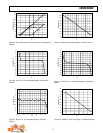
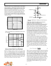
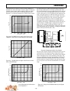
Figure 30 shows V
LOG
to be linear over a full 120 dB range.
Figure 31 shows the error ripple due to the individual gain func-
tions which is bounded by ±0.2 dB (dotted lines) from 6 µV to
2 V. The small perturbations at about 200 µV and 20 mV,
caused by the impracticality of matching the gain functions per-
fectly, are the only sign that the gains are now sequential. Fig-
ure 32 is a plot of V
AGC
which remains very close to its set value
of 316 mV rms over the full 120 dB range.
To more directly compare the signal-to-noise ratios in the
“simultaneous” and “sequential” modes of operation, all inter-
stage attenuation was eliminated (R2 and R3 in Figure 25, R2 in
Figure 29), the input of U1A was shorted, R5 was selected to
provide a 20 kHz bandwidth (R5 = 7.87 kΩ), and only the gain
control was varied, using an external source. The rms value of
the noise was then measured at V
OUT
and expressed as an S/N
5
3
–5
1µV10µV 10V1V100mV10mV1mV100µV
4
2
0
1
–1
–3
–2
–4
INPUT SIGNAL – V RMS
LOGARITHMIC OUTPUT – Volts
Figure 30. V
LOG
Is Essentially Linear Over the Full 120 dB
Range
ratio relative to 0 dBV, this being almost the maximum output
capability of the AD600. Results for the simultaneous mode can
be seen in Figure 33. The S/ N ratio degreades uniformly as the
gain is increased. Note that since the inverting gain control was
used, the gain in this curve and in Figure 34 decreases for more
positive values of the gain-control voltage.