


AD600/AD602
REV. A
–15–
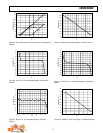
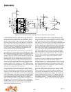
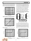
2.0
–2.0
1µV10µV 10V1V100mV10mV1mV100µV
0.5
1.0
1.5
–1.5
–1.0
–0.5
GAIN ERROR – dB
INPUT SIGNAL – V RMS
–0.1
0.1
0
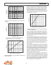
Figure 27. Gain Error for Figure 25 Without the 2 dB
Offset Modification
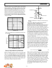
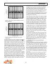
2.0
0
–2.0
1µV10µV 10V1V100mV10mV1mV100µV
0.5
1.0
1.5
–1.5
–1.0
–0.5
INPUT SIGNAL – V RMS
GAIN ERROR – dB
–0.1
0.1
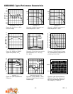
Figure 28. Adding the 2 dB Offsets Improves the
Linearization
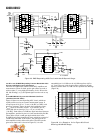
The maximum gain of this circuit is 120 dB. If no filtering were
used, the noise spectral density of the AD600 (1.4 nV/√
Hz)
would amount to an input noise of 8.28 µV rms in the full band-
width (35 MHz). At a gain of one million, the output noise
would dominate. Consequently, some reduction of bandwidth is
mandatory, and in the circuit of Figure 25 it is due mostly to a
single-pole low-pass filter R5/C3, which provides a –3 dB fre-
quency of 458 kHz, which reduces the worst-case output noise
(at V
AGC
) to about 100 mV rms at a gain of 100 dB. Of course,
the bandwidth (and hence output noise) could be easily reduced
further, for example, in audio applications, merely by increasing
C3. The value chosen for this application is optimal in minimiz-
ing the error in the V
LOG
output for small input signals.
The AD600 is dc-coupled, but even miniscule offset voltages at
the input would overload the output at high gains, so high-pass
filtering is also needed. To provide operation at low frequencies,
two simple zeros at about 12 Hz are provided by R1/C1 and
R4/C2; op amp sections U3A and U3B (AD713) are used to
provide impedance buffering, since the input resistance of the
AD600 is only 100 Ω. A further zero at 12 Hz is provided by C4
and the 6.7 kΩ input resistance of the AD636 rms converter.
The rms value of V
LOG
is generated at Pin 8 of the AD636; the
averaging time for this process is determined by C5, and the
value shown results in less than 1% rms error at 20 Hz. The
slowly varying V rms is compared with a fixed reference of
316 mV, derived from the positive supply by R10/R11. Any dif-
ference between these two voltages is integrated in C6, in con-
junction with op amp U3C, the output of which is V
LOG
. A
fraction of this voltage, determined by R12 and R13, is returned
to the gain control inputs of all AD600 sections. An increase in
V
LOG
lowers the gain, because this voltage is connected to the
inverting polarity control inputs.
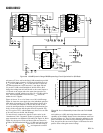
Now, in this case, the gains of all three VCA sections are being
varied simultaneously, so the scaling is not 32 dB/V but 96 dB/
V, or 10.42 mV/dB. The fraction of V
LOG
required to set its
scaling to 50 mV/dB is therefore 10.42/50, or 0.208. The result-
ing full-scale range of V
LOG
is nominally ±2.5 V. This scaling
was chosen to allow the circuit to operate from ±5 V supplies.
Optionally, the scaling could be altered to 100 mV/dB, which
would be more easily interpreted when V
LOG
is displayed on a
DVM, by increasing R12 to 25.5 kΩ. The full-scale output of
±5 V then requires the use of supply voltages of at least ±7.5 V.
A simple attenuator of 16.6 ± 1.25 dB is formed by R2/R3 and
the 100 Ω input resistance of the AD600. This allows the refer-
ence level of the decibel output to be precisely set to zero for an
input of 3.16 mV rms, and thus center the 100 dB range be-
tween 10 µV and 1 V. In many applications R2/R3 may be re-
placed by a fixed resistor of 590 Ω. For example, in AGC
applications, neither the slope nor the intercept of the logarith-
mic output is important.
A few additional components (R14–R16 and Q1) improve the
accuracy of V
LOG
at the top end of the signal range (that is, for
small gains). The gain starts rolling off when the input to the
first amplifier, U1A, reaches 0 dB. To compensate for this non-
linearity, Q1 turns on at V
LOG
~ +1.5 V and increases the feed-
back to the control inputs of the AD600s, thereby needing a
smaller voltage at V
LOG
to maintain the input to the AD636 to
the setpoint of 316 mV rms.
A 120 dB RMS/AGC System with Optimal S/N Ratio
(Sequential Gain)
In the last case, all gains were adjusted simultaneously, resulting
in an output signal-to-noise ratio (S/N ratio) which is always less
than optimal. The use of sequential gain control results in a ma-
jor improvement in S/N ratio, with only a slight penalty in the
accuracy of V
LOG
, and no penalty in the stabilization accuracy of
V
AGC
. The idea is simply to increase the gain of the earlier stages
first (as the signal level decreases) and thus maintain the highest
S/N ratio throughout the amplifier chain. This can be easily
achieved with the AD600 because its gain is accurate even when
the control input is overdriven; that is, each gaincontrol “win-
dow” of 1.25 V is used fully before moving to the next amplifier
to the right.
Figure 29 shows the circuit for the sequential control scheme.
R6 to R9 with R16 provide offsets of 42.14 dB between the
individual amplifiers to ensure smooth transitions between the
gain of each successive X-AMP, with the sequence of gain
increase being U1A first, then U1B, and lastly U2A. The adjust-
able attenuator provided by R3 + R17 and the 100 Ω input