


AD600/AD602
REV. A
–9–
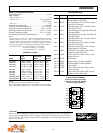
1
2
3
4
5
6
7
8
16
15
14
13
12
11
10
9
REF
A1
A2
C1HI
A1CM
A1OP
VPOS
VNEG
A2OP
A2CM
C2HI
C1LO
A1HI
A1LO
GAT1
GAT2
A2LO
A2HI
C2LO
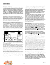
V
IN
+5V
100Ω
–5V
AD600 or AD602
100Ω
50Ω
V
OUT
GAIN-CONTROL
VOLTAGE
V
G
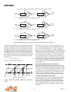
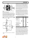
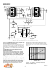
Figure 13. An Ultralow Noise VCA Using the AD600 or
AD602
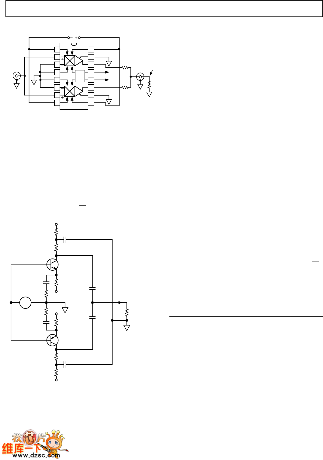
A Low Noise, 6 dB Preamplifier
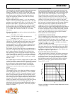
In some ultrasound applications, the user may wish to use a
high input impedance preamplifier to avoid the signal attenua-
tion that would result from loading the transducer by the 100 Ω
input resistance of the X-AMP. High gain cannot be tolerated,
because the peak transducer signal is typically ±0.5 V, while the
peak input capability of the AD600 or AD602 is only slightly
more than ±1 V. A gain of two is a suitable choice. It can be
shown that if the preamplifier’s overall referred-to-input (RTI)
noise is to be the same as that due to the X-AMP alone (1.4 nV/
√
Hz), then the input noise of a X2 preamplifier must be √(3/4)
times as large, that is, 1.2 nV/√
Hz.
INPUT
GROUND
0.1µF
0.1µF
100Ω
R OF X AMP
IN
OUTPUT
GROUND
Q2
MM4049
Q1
MRF904
1µF
1µF
–5V
+5V
V
IN
R4
42.2Ω
R5
42.2Ω
1µF
1µF
–5V
+5V
R1
49.9Ω
R2
174Ω
R3
562Ω
R6
562Ω
R7
174Ω
R8
49.9Ω
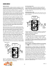
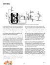
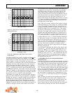
Figure 14. A Low Noise Preamplifier for the AD600 and
AD602
An inexpensive circuit, using complementary transistor types
chosen for their low r
bb
, is shown in Figure 14. The gain is de-
termined by the ratio of the net collector load resistance to the
net emitter resistance, that is, it is an open-loop amplifier. The
gain will be X2 (6 dB) only into a 100 Ω load, assumed to be
provided by the input resistance of the X-AMP; R2 and R7 are
in shunt with this load, and their value is important in defining
the gain. For small-signal inputs, both transistors contribute an
equal transconductance, which is rendered less sensitive to sig-
nal level by the emitter resistors R4 and R5, which also play a
dominant role in setting the gain.
This is a Class AB amplifier. As V
IN
increases in a positive di-
rection, Q1 conducts more heavily and its r
e
becomes lower
while that of Q2 increases. Conversely, more negative values of
V
IN
result in the r
e
Of Q2 decreasing, while that of Q1 increases.
The design is chosen such that the net emitter resistance is es-
sentially independent of the instantaneous value of V
IN
, result-
ing in moderately low distortion. Low values of resistance and
moderately high bias currents are important in achieving the low
noise, wide bandwidth, and low distortion of this preamplifier.
Heavy decoupling prevents noise on the power supply lines from
being conveyed to the input of the X-AMP.
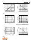
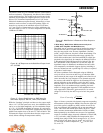
Table I. Measured Preamplifier Performance
Measurement Value Unit
Gain (f = 30 MHz) 6 dB
Bandwidth (–3 dB) 250 MHz
Input Signal for
1 dB Compression 1 V p-p
Distortion
V
IN
= 200 mV p-p HD2 0.27 %
HD3 0.14 %
V
IN
= 500 mV p-p HD2 0.44 %
HD3 0.58 %
System Input Noise 1.03 nV/√
Hz
Spectral Density (NSD)
(Preamp plus X-AMP)
Input Resistance 1.4 kΩ
Input Capacitance 15 pF
Input Bias Current ±150 µA
Power Supply Voltage ±5V
Quiescent Current 15 mA
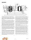
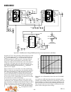
A Low Noise AGC Amplifier with 80 dB Gain Range
Figure 15 provides an example of the ease with which the
AD600 can be connected as an AGC amplifier. A1 and A2 are
cascaded, with 6 dB of attenuation introduced by the 100 Ω
resistor R1, while a time constant of 5 ns is formed by C1 and
the 50 Ω of net resistance at the input of A2. This has the dual
effect of (a) lowering the overall gain range from {0 dB to 80 dB}
to {6 dB to 74 dB} and (b) introducing a single-pole low-pass
filter with a –3 dB frequency of about 32 MHz. This ensures
stability at the maximum gain for a slight reduction in the over-
all bandwidth. The capacitor C4 blocks the small dc offset volt-
age at the output of A1 (which might otherwise saturate A2 at
its maximum gain) and introduces a high pass corner at about
8 kHz, useful in eliminating low frequency noise and spurious
signals which may be present at the input.