


AD600/AD602
REV. A
–17–
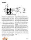
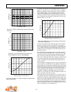
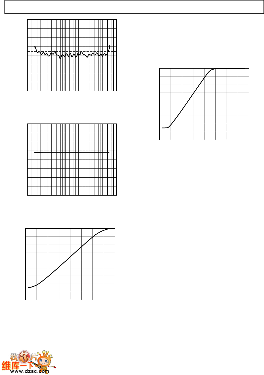
2.0
0
–2.0
1µV10µV 10V1V100mV10mV1mV100µV
0.5
1.0
1.5
–1.5
–1.0
–0.5
INPUT SIGNAL – V RMS
GAIN ERROR – dB
0.2
–0.2
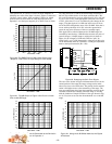
Figure 31. The Error Ripple Due to the Individual Gain
Functions
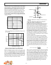
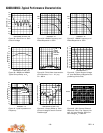
400
300
200
1µV10µV 10V1V100mV10mV1mV100µV
350
250
INPUT SIGNAL – V RMS
GAIN ERROR – mV
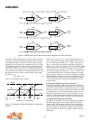
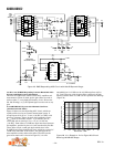
Figure 32. V
AGC
Remains Nose to Its Setpoint of
316 mV RMS Over the Full 120 dB Range
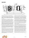
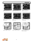
90
0
833.2
20
10
–625.0–833.2
30
40
50
60
70
80
625.0416.6208.3
0
–208.3–416.6
CONTROL VOLTAGE, V (10.417mV/dB) – mV
C
S/N RATIO – dB
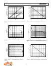
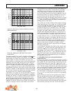
Figure 33. S/N Ratio vs. Control Voltage for Parallel Gain
Control (Figure 25)
In contrast, the S/N ratio for the sequential mode is shown in
Figure 34. U1A always acts as a fixed noise source; varying its
gain has no influence on the output noise. (This is a feature of
the X-AMP technique.) Thus, for the first 40 dB of control
range (actually slightly more, as explained below), when only
this VCA section has its gain varied, the S/N ratio remains con-
stant. During this time, the gains of U1B and U2A are at their
minimum value of –1.07 dB.
90
0
3.817
20
10
–0.558–1.183
30
40
50
60
70
80
3.1922.5671.9421.3170.6920.067
CONTROL VOLTAGE, V (31.25mV/dB) – Volts
C
S/N RATIO – dB
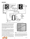
Figure 34. S/N Ratio vs. Control Voltage for Sequential
Gain Control (Figure 29)
For the next 40 dB of control range, the gain of U1A remains
fixed at its maximum value of 41.07 dB and only the gain of
U1B is varied, while that of U2A remains at its minimum value
of –1.07 dB. In this interval, the fixed output noise of U1A is
amplified by the increasing gain of U1B and the S/N ratio pro-
gressively decreases.
Once U1B reaches its maximum gain of 41.07 dB, its output
also becomes a gain independent noise source; this noise is pre-
sented to U2A. As the control voltage is further increased, the
gains of both U1A and U1B remain fixed at their maximum
value of 41.07 dB, and the S/N ratio continues to decrease. Fig-
ure 34 clearly shows this, because the maximum S/N ratio of
90 dB is extended for the first 40 dB of input signal before it
starts to roll off.
This arrangement of staggered gains can be easily implemented
because, when the control inputs of the AD600 are overdriven,
the gain limits to its maximum or minimum values without side
effects. This eliminates the need for awkward nonlinear shaping
circuits that have previously been used to break up the gain
range of multistage AGC amplifiers. It is the precise values of
the AD600’s maximum and minimum gain (not 0 dB and
40 dB but –1.07 dB and 41.07 dB) that explain the rather odd
values of the offset values that are used.
The optimization of the output S/N ratio is of obvious value in
AGC systems. However, in applications where these circuit are
considered for their wide range logarithmic measurements capa-
bilities, the inevitable degradation of the S/N ratio at high gains
need not seriously impair their utility. In fact, the bandwidth of
the circuit shown in Figure 25 was specifically chosen so as to
improve measurement accuracy by altering the shape of the log
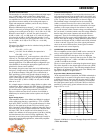
error curve (Figure 31) at low signal levels.