


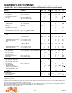

AD600/AD602
REV. A
–5–
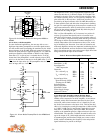
The Gain-Control Interface
The attenuation is controlled through a differential, high imped-
ance (15 MΩ) input, with a scaling factor which is laser
trimmed to 32 dB per volt, that is, 31.25 mV/dB. Each of the
two amplifiers has its own control interface. An internal band-
gap reference ensures stability of the scaling with respect to
supply and temperature variations, and is the only circuitry
common to both channels.
When the differential input voltage V
G
= 0 V, the attenuator
“slider” is centered, providing an attenuation of 21.07 dB, thus
resulting in an overall gain of 20 dB (= –21.07 dB + 41.07 dB).
When the control input is –625 mV, the gain is lowered by
20 dB (= 0.625 × 32), to 0 dB; when set to +625 mV, the gain
is increased by 20 dB, to 40 dB. When this interface is over-
driven in either direction, the gain approaches either –1.07 dB
(= –42.14 dB + 41.07 dB) or 41.07 dB (= 0 + 41.07 dB),
respectively.
The gain of the AD600 can thus be calculated using the follow-
ing simple expression:
Gain (dB) = 32 V
G
+ 20 (1)
where V
G
is in volts. For the AD602, the expression is:
Gain (dB) = 32 V
G
+ 10 (2)
Operation is specified for V
G
in the range from –625 mV dc to
+625 mV dc. The high impedance gain-control input ensures
minimal loading when driving many amplifiers in multiple-
channel applications. The differential input configuration pro-
vides flexibility in choosing the appropriate signal levels and
polarities for various control schemes.
For example, the gain-control input can be fed differentially to
the inputs, or single-ended by simply grounding the unused in-
put. In another example, if the gain is to be controlled by a
DAC providing a positive only ground referenced output, the
“Gain Control LO” pin (either C1LO or C2LO) should be bi-
ased to a fixed offset of +625 mV, to set the gain to 0 dB when
“Gain Control HI” (C1HI or C2HI) is at zero, and to 40 dB
when at +1.25 V.
It is a simple matter to include a voltage divider to achieve other
scaling factors. When using an 8-bit DAC having a FS output of
+2.55 V (10 mV/bit) a divider ratio of 1.6 (generating 6.25 mV/
bit) would result in a gain setting resolution of 0.2 dB/ bit.
Later, we will discuss how the two sections of an AD600 or
AD602 may be cascaded, when various options exist for gain
control.
Signal-Gating Inputs
Each amplifier section of the AD600 and AD602 is equipped
with a signal gating function, controlled by a TTL or CMOS
logic input (GAT1 or GAT2). The ground references for these
inputs are the signal input grounds A1LO and A2LO, respec-
tively. Operation of the channel is unaffected when this input is
LO or left open-circuited. Signal transmission is blocked when
this input is HI. The dc output level of the channel is set to
within a few millivolts of the output ground (A1CM or A2CM),
and simultaneously the noise level drops significantly. The
reduction in noise and spurious signal feedthrough is useful in
ultrasound beam-forming applications, where many amplifier
outputs are summed.
Common-Mode Rejection
A special circuit technique is used to provide rejection of volt-
ages appearing between input grounds (A1LO and A2LO) and
output grounds (A1CM and A2CM). This is necessary because
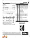
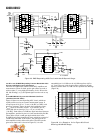
of the “op amp” form of the amplifier, as shown in Figure 1.
The feedback voltage is developed across the resistor RF1
(which, to achieve low noise, has a value of only 20 Ω). The
voltage developed across this resistor is referenced to the input
common, so the output voltage is also referred to that node.
To provide rejection of this common voltage, an auxiliary ampli-
fier (not shown) is included, which senses the voltage difference
between input and output commons and cancels this error
component. Thus, for zero differential signal input between
A1HI and A1LO, the output A1OP simply follows the voltage at
A1CM. Note that the range of voltage differences which can ex-
ist between A1LO and A1CM (or A2LO and A2CM) is limited
to about ±100 mV. Figure 50 (one of the typical performance
curves at the end of this data sheet) shows typical common-
mode rejection ratio versus frequency.
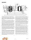
ACHIEVING 80 dB GAIN RANGE
The two amplifier sections of the X-AMP can be connected in
series to achieve higher gain. In this mode, the output of A1
(A1OP and A1CM) drives the input of A2 via a high-pass
network (usually just a capacitor) that rejects the dc offset. The
nominal gain range is now –2 dB to +82 dB for the AD600 or
–22 dB to +62 dB for the AD602.
There are several options in connecting the gain-control inputs.
The choice depends on the desired signal-to-noise ratio (SNR)
and gain error (output ripple). The following examples feature
the AD600; the arguments generally apply to the AD602, with
appropriate changes to the gain values.
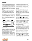
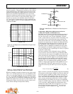
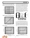
Sequential Mode (Maximum S/N Ratio)
In the sequential mode of operation, the SNR is maintained at
its highest level for as much of the gain control range possible,
as shown in Figure 2. Note here that the gain range is 0 dB to
80 dB. Figure 3 shows the general connections to accomplish
this. Both gain-control inputs, C1HI and C2HI, are driven in
parallel by a positive only, ground referenced source with a
range of 0 V to +2.5 V.
V
G
S/N RATIO – dB
85
30
3.0
45
35
0.0
40
–0.5
60
50
55
65
70
75
80
2.52.01.51.00.5
Figure 2. S/N Ratio vs. Control Voltage Sequential Control
(1 MHz Bandwidth)