


AD600/AD602
REV. A
–13–
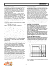
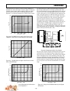
(This system can, of course, be used as an AGC amplifier, in
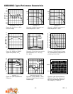
which the rms value of the input is leveled.) Figure 21 shows the
“decibel” output voltage. More revealing is Figure 22, which
shows that the deviation from the ideal output predicted by
Equation 1 over the input range 80 µV to 500 mV rms is within
450
300
150
10µV 100µV 10V1V100mV10mV1mV
225
375
350
200
275
425
325
175
250
400
INPUT SIGNAL –V RMS
V – mV
OUT
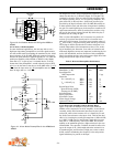
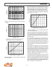
Figure 20. The RMS Output of A2 Is Held Close to the
“Setpoint” 316 mV for an Input Range of Over 80 dB
5
0
–5
10µV 100µV 10V1V100mV10mV1mV
1
2
3
4
–4
–3
–2
–1
INPUT SIGNAL – V RMS
V – Volts
OUT
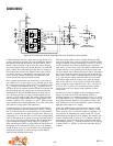
Figure 21. The dB Output of Figure 19’s Circuit Is Linear
Over an 80 dB Range
2.5
0
–2.5
10µV 100µV 10V1V100mV10mV1mV
0.5
1.0
1.5
2.0
–2.0
–1.5
–1.0
–0.5
INPUT SIGNAL – V RMS
OUTPUT ERROR – dB
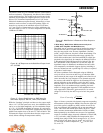
Figure 22. Data from Figure 20 Presented as the Deviation
from the Ideal Output Given in Equation 4
±0.5 dB, and within ±1 dB for the 80 dB range from 80 µV to
800 mV. By suitable choice of the input attenuator R1 + R2,
this could be centered to cover any range from 25 mV to 250 mV
to, say, 1 mV to 10 V, with appropriate correction to the value
of V
REF
. (Note that V
SCALE
is not affected by the changes in the
range.) The gain ripple of ±0.2 dB seen in this curve is the re-
sult of the finite interpolation error of the X-AMP. Note that it
occurs with a periodicity of 12 dB—twice the separation be-
tween the tap points (because of the two cascaded stages).
This ripple can be canceled whenever the X-AMP stages are
cascaded by introducing a 3 dB offset between the two pairs of
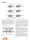
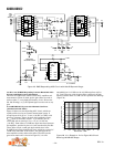
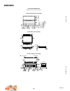
control voltages. A simple means to achieve this is shown in
Figure 23: the voltages at C1HI and C2HI are “split” by
±46.875 mV, or ±1.5 dB. Alternatively, either one of these pins
can be individually offset by 3 dB and a 1.5 dB gain adjustment
made at the input attenuator (R1 + R2).
16
15
14
13
12
11
10
9
C1HI
A1CM
A1OP
VPOS
VNEG
A2OP
A2CM
C2HI
+6V DEC
–6V DEC
C2
2µF
1
2
3
4
5
6
7
NC
NC
NC
–6V
DEC
VINP
VNEG
CAVG
VLOG
BFOP
BFIN
U2
AD636
U1
AD600
–46.875mV +46.875mV
NC = NO CONNECT
10kΩ 78.7Ω 78.7Ω 10kΩ
+6V
DEC
3dB OFFSET
MODIFICATION
–6V
DEC
Figure 23. Reducing the Gain Error Ripple
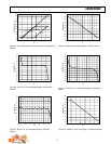
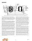
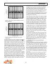
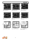
The error curve shown in Figure 24 demonstrates that over the
central portion of the range the output voltage can be main-
tained very close to the ideal value. The penalty for this modifi-
cation is the higher errors at the extremities of the range. The
next two applications show how three amplifier sections can be
cascaded to extend the nominal conversion range to 120 dB,
with the inclusion of simple LP filters of the type shown in Fig-
ure 15. Very low errors can then be maintained over a 100 dB
range.
2.5
0
–2.5
10µV 100µV 10V1V100mV10mV1mV
0.5
1.0
1.5
2.0
–2.0
–1.5
–1.0
–0.5
INPUT SIGNAL – V RMS
OUTPUT ERROR – dB
Figure 24. Using the 3 dB Offset Network, the Ripple
Is Reduced