


AD600/AD602
REV. A
–6–
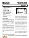
41.07dB
–40.00dB
C1HI C1LO
V = 0.592V
O1
1.07dB
41.07dB
–42.14dB
C1HI C1LO
V = 1.908V
O2
V
G1
V
G2
OUTPUT
0dB
–41.07dB
–40.00dB
INPUT
0dB
V = 0V
C
41.07dB
–0.51dB
C1HI C1LO
V = 0.592V
O1
40.56dB
41.07dB
–41.63dB
C1HI C1LO
V = 1.908V
O2
V
G1
V
G2
OUTPUT
40dB
–1.07dB–0.51dB
INPUT
0dB
V = 1.25V
C
41.07dB
0dB
C1HI C1LO
V = 0.592V
O1
41.07dB
41.07dB
–2.14dB
C1HI C1LO
V = 1.908V
O2
V
G1
V
G2
OUTPUT
80dB
38.93dB0dB
INPUT
0dB
V = 25V
C
A1 A2
(a)
(b)
(c)
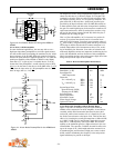
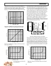
Figure 3. AD600 Gain Control Input Calculations for Sequential Control Operation
When V
C
is set to zero, V
G1
= –0.592 V and the gain of A1 is
+1.07 dB (recall that the gain of each amplifier section is 0 dB
for V
G
= 625 mV); meanwhile, V
G2
= –1.908 V so the gain of
A2 is –1.07 dB. The overall gain is thus 0 dB (see Figure 3a).
When V
C
= +1.25 V, V
G1
= 1.25 V– 0.592 V = +0.658 V, which
sets the gain of A1 to 40.56 dB, while V
G2
= 1.25 V – 1.908 V =
–0.658 V, which sets A2’s gain at –0.56 dB. The overall gain is
now 40 dB (see Figure 3b). When V
C
= +2.5 V, the gain of A1
is 41.07 dB and that of A2 is 38.93 dB, resulting in an overall
gain of 80 dB (see Figure 3c). This mode of operation is further
clarified by Figure 5, which is a plot of the separate gains of A1
and A2 and the overall gain versus the control voltage. Figure 6
is a plot of the gain error of the cascaded amplifiers versus the
control voltage.
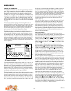
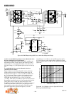
Parallel Mode (Simplest Gain-Control Interface)
In this mode, the gain-control voltage is applied to both inputs
in parallel—C1HI and C2HI are connected to the control volt-
age, and C1LO and C2LO are optionally connected to an offset
voltage of +0.625 V. The gain scaling is then doubled to 64 dB/
V, requiring only 1.25 V for an 80 dB change of gain. The am-
plitude of the gain ripple in this case is also doubled, as shown
in Figure 7, and the instantaneous signal-to-noise ratio at the
output of A2 decreases linearly as the gain is increased (Figure 8).
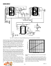
Low Ripple Mode (Minimum Gain Error)
As can be seen in Figures 6 and 7, the output ripple is periodic.
By offsetting the gains of Al and A2 by half the period of the
ripple, or 3 dB, the residual gain errors of the two amplifiers
can be made to cancel. Figure 9 shows the much lower gain rip
ple when configured in this manner. Figure 10 plots the S/N
ratio as a function of gain; it is very similar to that in the “Par-
allel Mode.”
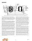
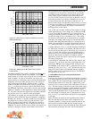
The gains are offset (Figure 4) such that A2’s gain is increased
only after A1’s gain has reached its maximum value. Note that
for a differential input of –700 mV or less, the gain of a single
amplifier (A1 or A2) will be at its minimum value of –1.07 dB;
for a differential input of +700 mV or more, the gain will be at
its maximum value of 41.07 dB. Control inputs beyond these
limits will not affect the gain and can be tolerated without dam-
age or foldover in the response. See the Specifications Section of
this data sheet for more details on the allowable voltage range.
The gain is now
Gain (dB) = 32 V
C
(3)
where V
C
is the applied control voltage.
+41.07dB
20dB
+1.07dB
–0.56dB
–1.07dB
40.56dB +38.93dB
0.592 1.908
A1 A2
0 0.625 1.25 1.875
2.5
020406080–2.14 82.14
GAIN
(dB)
*GAIN OFFSET OF 1.07dB, OR 33.44mV
*
*
C
V (V)
Figure 4. Explanation of Offset Calibration for Sequential
Control