


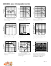
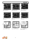

AD600/AD602
REV. A
–12–
INPUT
1V RMS
MAX
(SINE WAVE)
0.1µF
0.1µF
FB
–6V
+6V
POWER SUPPLY
DECOUPLING NETWORK
+6V DEC
–6V DEC
1
2
3
4
5
6
7
8
16
15
14
13
12
11
10
9
REF
A1
A2
C1HI
A1CM
A1OP
VPOS
VNEG
A2OP
A2CM
C2HI
C1LO
A1HI
A1LO
GAT1
GAT2
A2LO
A2HI
C2LO
R3
133kΩ
R2 200Ω
U1 AD600
+6V DEC
–6V DEC
C2
2µF
C1
0.1µF
U3A
1/2
AD712
R1
115Ω
CAL 0dB
C4
4.7µF
R5
16.2kΩ
1
2
3
4
5
6
7
14
13
12
11
10
9
8
NC
NC
NC
–6V DEC
U3B
R6
3.16kΩ
R7
56.2kΩ
+6V DEC
NC
NC
NC
V
OUT
+100mV/dB
0V = 0dB (AT 10mV RMS)
R4
3.01kΩ
1/2
AD712
V
15.625mV/dB
G
+316.2mV
C3
1µF
VINP
VNEG
CAVG
VLOG
BFOP
BFIN
VPOS
COMM
LDLO
VRMS
U2
AD636
AF/RF
OUTPUT
NC = NO CONNECT
V
RMS
FB
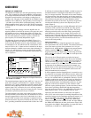
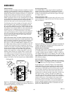
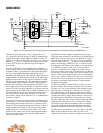
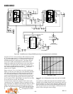
Figure 19. The Output of This Three-IC Circuit Is Proportional to the Decibel Value of the RMS Input
Note that the peak “log output” of ±4 V requires the use of
±6 V supplies for the dual op amp U3 (AD712) although lower
supplies would suffice for the AD600 and AD636. If only ±5 V
supplies are available, it will be either necessary to use a reduced
value for V
SCALE
(say 1 V, in which case the peak output would
be only ±2 V) or restrict the dynamic range of the signal to
about 60 dB.
As in the previous case, the two amplifiers of the AD600 are
used in cascade. However, the 6 dB attenuator and low-pass fil-
ter found in Figure 1 are replaced by a unity gain buffer ampli-
fier U3A, whose 4 MHz bandwidth eliminates the risk of
instability at the highest gains. The buffer also allows the use of
a high impedance coupling network (C1/R3) which introduces a
high-pass corner at about 12 Hz. An input attenuator of 10 dB
(X0.316) is now provided by R1 + R2 operating in conjunction
with the AD600’s input resistance of 100 Ω. The adjustment
provides exact calibration of the logarithmic intercept V
REF
in
critical applications, but R1 and R2 may be replaced by a fixed
resistor of 215 Ω if very close calibration is not needed, since the
input resistance of the AD600 (and all other key parameters of it
and the AD636) are already laser trimmed for accurate opera-
tion. This attenuator allows inputs as large as ±4 V to be ac-
cepted, that is, signals with an rms value of 1 V combined with a
crest factor of up to 4.
The output of A2 is ac coupled via another 12 Hz high-pass fil-
ter formed by C2 and the 6.7 kΩ input resistance of the AD636.
The averaging time constant for the rms-dc converter is deter-
mined by C4. The unbuffered output of the AD636 (at Pin 8) is
compared with a fixed voltage of +316 mV set by the positive
supply voltage of +6 V and resistors R6 and R7. (V
REF
is pro-
portional to this voltage, and systems requiring greater calibra-
tion accuracy should replace the supply dependent reference
with a more stable source.)
Any difference in these voltages is integrated by the op amp
U3B, with a time constant of 3 ms formed by the parallel sum of
R6/R7 and C3. Now, if the output of the AD600 is too high, V
rms will be greater than the “setpoint” of 316 mV, causing the
output of U3B—that is, V
OUT
—to ramp up (note that the inte-
grator is noninverting). A fraction of V
OUT
is connected to the
inverting gain-control inputs of the AD600, so causing the gain
to be reduced, as required, until V rms is exactly equal to
316 mV, at which time the ac voltage at the output of A2 is
forced to be exactly 316 mV rms. This fraction is set by R4 and
R5 such that a 15.625 mV change in the control voltages of A1
and A2—which would change the gain of the cascaded amplifi-
ers by 1 dB—requires a change of 100 mV at V
OUT
. Notice here
that since A2 is forced to operate at an output level well below
its capacity, waveforms of high crest factor can be tolerated
throughout the amplifier.
To check the operation, assume an input of 10 mV rms is ap-
plied to the input, which results in a voltage of 3.16 mV rms at
the input to A1, due to the 10 dB loss in the attenuator. If the
system operates as claimed, V
OUT
(and hence V
G
) should be
zero. This being the case, the gain of both A1 and A2 will be
20 dB and the output of the AD600 will therefore be 100 times
(40 dB) greater than its input, which evaluates to 316 mV rms,
the input required at the AD636 to balance the loop. Finally,
note that unlike most AGC circuits, needing strong temperature
compensation for the internal “kT/q” scaling, these voltages,
and thus the output of this measurement system, are tempera-
ture stable, arising directly from the fundamental and exact
exponential attenuation of the ladder networks in the AD600.
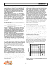
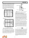
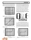
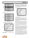
Typical results are presented for a sine wave input at 100 kHz.
Figure 20 shows that the output is held very close to the
setpoint of 316 mV rms over an input range in excess of 80 dB.