


Electrical Requirements
R
24 mPGA604 Socket Design Guidelines
4.2 Determination of Maximum Electrical Resistance
This section provides a guideline for the instruments used to take the measurements.
Note: The instrument selection should consider the guidelines in EIA 364-23A.
1. These measurements use a 4-wire technique, where the instruments provide two separate
circuits. One is a precision current source to deliver the test current. The other is a precision
voltmeter circuit to measure the voltage drop between the desired points.
2. These separate circuits can be contained within one instrument, such as a high quality micro-
ohmmeter, a stand-alone current source and voltmeter, or the circuits of a data acquisition
system.
3. Measurement accuracy in Ω is specified as ± 0.1% of reading, or ± 0.1 m Ω, whichever is
greater. The vendor is responsible for demonstrating that their instrument(s) can meet this
accuracy.
4. Automation of the measurements can be implemented by scanning the chains through the
edge or cable test connector using a switch matrix. The matrix can be operated by hand, or
through software.
5. Measure R
Total
for each daisy chain of “package + socket + motherboard” unit.
6. Measure R
jumper
for each daisy chain of 30 “package + motherboard” units. Calculate
jumper
R for each daisy chain (There is 30 data for each daisy chain).
7. For each socket unit, calculate
N
RR
R
jumper
Total
Req
−
=
R
Req
is the average contact resistance for socket pin.
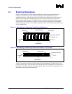
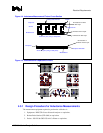
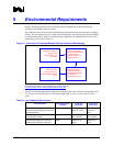
4.3 Inductance
The bottom fixture for the inductance measurement is a ground plane on the secondary side of the
motherboard with all pins grounded. The component side of the socket PCB does not contain a
plane. The top fixture is the package, which contains pins that will connect to the socket. Figure 4-4
shows the inductance measurement fixture cross-section and the inductance measurement
methodology. The first figure shows the entire assembly. The second figure shows the assembly
without the socket; the socket-seating plane of the package is directly mounted to the component
side of the socket PCB. This is used to calibrate out the fixture contribution. The materials for the
fixture must match the materials used in the processor. Note the probe pad features exist on the
topside of the top fixture, and the shorting plane exists only on the bottom side of the bottom fixture.
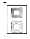
Figure 4-5 presents the inductance and capacitance fixture design.