


36 CY4672 Reference Design Guide, Document # 001-16968 Revision **
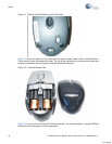
Mouse
test mode that is compatible with the Cypress Manufacturing Test Kit, use a shorting block and short
together pins 4 and 5 before power is applied.
3.2.4 Hardware Considerations
The mouse design uses the SS12 schottky diode (D1) and CDH53100LC inductor (L3) for its boost
circuitry. With these high efficiency components, preliminary characterization data shows a range of
approximately 74-87% efficiency for the 1.8-2.7V VBAT voltage range at different temperatures
(-10C to 80C). The mouse is a higher power consumption device compared to the keyboard. Extend-
ing the battery life is one of the crucial design considerations in the mouse design. The trade off for a
higher efficiency boost circuitry is the component costs and the board size (these components are
slightly bigger in size compared to the ones used in the keyboard design). These components do not
provide enough current capacity at the low end of the VBAT voltage range to handle the worst case
optical sensor load and the PMU output voltage may droop under these conditions. The recommen-
dation is to use an external DC/DC boost circuit for the optical system only.
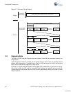
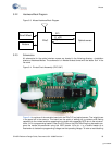
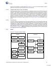
3.3 Firmware Architecture
There are two architectural views of the mouse. The first is a microcontroller configuration view. This
architecture and configuration is best viewed in the PSoC Designer™ application when the project is
loaded. The second view is a logical organization of the source code modules that make up the
mouse application code and other support modules.
This section describes both architectures with emphasis on top level organization and overall mod-
ule operation. More detailed description of variables and functions should be obtained by studying
the source code.
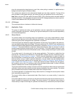
3.3.1 ROM/RAM Usage
The following table shows the ROM/RAM usage. The top part exhibits the total ROM/RAM usage for
basic functions, which disables all the build options below. The bottom part exhibits the ROM/RAM
usage for individual build options.
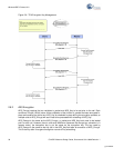
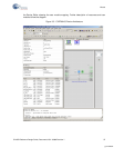
3.3.2 PRoC LP Device Configuration
The PRoC LP Programmable Radio on Chip is configured using the Device Editor in PSoC
Designer. The mouse uses 2 digital blocks to support two separate user modules. The first module is
an SPI master for communicating with the optical sensor and the radio. The second module is a Pro-
grammable Interval Timer configured to operate as a 12-bit timer. The following is a screen shot of
Table 3-1. ROM/RAM Usage
Total ROM (Bytes) Total RAM (Bytes)
Basic Function 5334 70
Build Option ROM Usage (Bytes) RAM Usage (Bytes)
MOUSE_BATTERY_STATUS 255 2
MOUSE_TEST_MODE 537 0
MFG_TEST_CODE 530 0
MFG_TX_MODES 755 2
[+] Feedback