


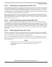

ESAI Programming Model
DSP56364 24-Bit Digital Signal Processor Users Manual, Rev. 2
Freescale Semiconductor 6-41
6.3.7 ESAI Receive Shift Registers
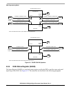
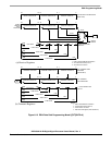
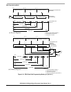
The receive shift registers (see Figure 6-13 and Figure 6-14) receive the incoming data from the serial
receive data pins. Data is shifted in by the selected (internal/external) bit clock when the associated frame
sync I/O is asserted. Data is assumed to be received MSB first if RSHFD=0 and LSB first if RSHFD=1.
Data is transferred to the ESAI receive data registers after 8, 12, 16, 20, 24, or 32 serial clock cycles were
counted, depending on the slot length control bits in the RCR register.
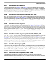
6.3.8 ESAI Receive Data Registers (RX3, RX2, RX1, RX0)
RX3, RX2, RX1 and RX0 are 24-bit read-only registers that accept data from the receive shift registers
when they become full (see Figure 6-13 and Figure 6-14). The data occupies the most significant portion
of the receive data registers, according to the ALC control bit setting. The unused bits (least significant
portion, and 8 most significant bits when ALC=1) read as zeros. The DSP is interrupted whenever RXx
becomes full if the associated interrupt is enabled.
6.3.9 ESAI Transmit Shift Registers
The transmit shift registers contain the data being transmitted (see Figure 6-13 and Figure 6-14). Data is
shifted out to the serial transmit data pins by the selected (internal/external) bit clock when the associated
frame sync I/O is asserted. The number of bits shifted out before the shift registers are considered empty
and may be written to again can be 8, 12, 16, 20, 24 or 32 bits (determined by the slot length control bits
in the TCR register). Data is shifted out of these registers MSB first if TSHFD=0 and LSB first if
TSHFD=1.
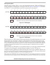
6.3.10 ESAI Transmit Data Registers (TX5, TX4, TX3, TX2,TX1,TX0)
TX5, TX4, TX3, TX2, TX1 and TX0 are 24-bit write-only registers. Data to be transmitted is written into
these registers and is automatically transferred to the transmit shift registers (see Figure 6-13 and
Figure 6-14). The data written (8, 12, 16, 20 or 24 bits) should occupy the most significant portion of the
TXx according to the ALC control bit setting. The unused bits (least significant portion, and the 8 most
significant bits when ALC=1) of the TXx are don’t care bits. The DSP is interrupted whenever the TXx
becomes empty if the transmit data register empty interrupt has been enabled.
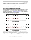
6.3.11 ESAI Time Slot Register (TSR)
The write-only Time Slot Register (TSR) is effectively a null data register that is used when the data is not
to be transmitted in the available transmit time slot. The transmit data pins of all the enabled transmitters
are in the high-impedance state for the respective time slot where TSR has been written. The Transmitter
External Buffer Enable pin (FSR pin when SYN=1, TEBE=1, RFSD=1) disables the external buffers
during the slot when the TSR register has been written.
6.3.12 Transmit Slot Mask Registers (TSMA, TSMB)
The Transmit Slot Mask Registers (TSMA and TSMB) are two read/write registers used by the
transmitters in network mode to determine for each slot whether to transmit a data word and generate a