


Core Description
DSP56364 24-Bit Digital Signal Processor Users Manual, Rev. 2
1-4 Freescale Semiconductor
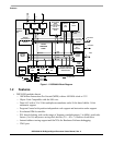
1.4 Core Description
The DSP56364 uses the DSP56300 core, a high-performance, single clock cycle per instruction engine that
provides up to twice the performance of Freescale's popular DSP56000 core family while retaining code
compatibility with it.
The DSP56300 core provides the following functional blocks:
• Data arithmetic logic unit (Data ALU)
• Address generation unit (AGU)
• Program control unit (PCU)
• Bus interface unit (BIU)
• DMA controller (with six channels)
• Instruction cache controller
• PLL-based clock oscillator
• OnCE module
• JTAG TAP
• Memory
The DSP56300 core family offers a new level of performance in speed and power, provided by its rich
instruction set and low power dissipation, thus enabling a new generation of wireless, telecommunications,
and multimedia products. Significant architectural enhancements to the DSP56300 core family include a
barrel shifter, 24-bit addressing, an instruction cache, and direct memory access (DMA).
Core features are described fully in the DSP56300 Family Manual. Pinout, memory, and peripheral
features are described in this manual.
1.5 DSP56300 Core Functional Blocks
1.5.1 Data ALU
The Data ALU performs all the arithmetic and logical operations on data operands in the DSP56300 core.
The components of the Data ALU are as follows:
• Fully pipelined 24-bit × 24-bit parallel multiplier-accumulator (MAC)
• Bit field unit, comprising a 56-bit parallel barrel shifter (fast shift and normalization; bit stream
generation and parsing)
• Conditional ALU instructions
• 24-bit or 16-bit arithmetic support under software control
• Four 24-bit input general purpose registers: X1, X0, Y1, and Y0
• Six Data ALU registers (A2, A1, A0, B2, B1, and B0) that are concatenated into two general
purpose, 56-bit accumulators (A and B), accumulator shifters
• Two data bus shifter/limiter circuits