


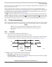

SHI Programming Considerations
DSP56364 24-Bit Digital Signal Processor Users Manual, Rev. 2
7-22 Freescale Semiconductor
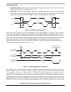
• SCK/SCL is the SCL serial clock input.
• MISO/SDA is the SDA open drain serial data line.
• MOSI/HA0 is the HA0 slave device address input.
•SS/HA2 is the HA2 slave device address input.
•HREQ
is the Host Request output.
When the SHI is enabled and configured in the I
2
C Slave mode, the SHI controller inspects the SDA and
SCL lines to detect a start event. Upon detection of the start event, the SHI receives the slave device
address byte and enables the slave device address recognition unit. If the slave device address byte was not
identified as its personal address, the SHI controller will fail to acknowledge this byte by not driving low
the SDA line at the ninth clock pulse (ACK = 1). However, it continues to poll the SDA and SCL lines to
detect a new start event. If the personal slave device address was correctly identified, the slave device
address byte is acknowledged (ACK = 0 is sent) and a receive/transmit session is initiated according to the
eighth bit of the received slave device address byte (i.e., the R/W bit).
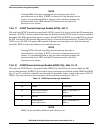
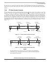
7.7.3.1 Receive Data in I
2
C Slave Mode
A receive session is initiated when the personal slave device address has been correctly identified and the
R/W bit of the received slave device address byte has been cleared. Following a receive initiation, data in
the SDA line is shifted into IOSR MSB first. Following each received byte, an acknowledge (ACK = 0) is
sent at the ninth clock pulse via the SDA line. Data is acknowledged bytewise, as required by the I
2
C bus
protocol, and is transferred to the HRX FIFO when the complete word (according to HM0–HM1) is filled
into IOSR. It is the responsibility of the programmer to select the correct number of bytes in an I
2
C frame
so that they fit in a complete number of words. For this purpose, the slave device address byte does not
count as part of the data, and therefore, it is treated separately.
In a receive session, only the receive path is enabled and HTX to IOSR transfers are inhibited. The HRX
FIFO contains valid data, which may be read by the DSP using either DSP instructions or DMA transfers
if the HRNE status bit is set.
If HCKFR is cleared, when the HRX FIFO is full and IOSR is filled, an overrun error occurs and the HROE
status bit is set. In this case, the last received byte will not be acknowledged (ACK = 1 is sent) and the
word in the IOSR will not be transferred to the HRX FIFO. This may inform the external I
2
C master device
of the occurrence of an overrun error on the slave side. Consequently the I
2
C master device may terminate
this session by generating a stop event.
If HCKFR is set, when the HRX FIFO is full the SHI will hold the clock line to GND not letting the master
device write to IOSR. This effectively eliminates the possibility of reaching the overrun condition.
The HREQ
output pin, if enabled for receive (HRQE1–HRQE0 = 01), is asserted when the IOSR is ready
to receive and the HRX FIFO is not full; this operation guarantees that the next received data word will be
stored in the FIFO. HREQ
is deasserted at the first clock pulse of the next received word. The HREQ line
may be used to interrupt the external I
2
C master device. Connecting the HREQ line between two
SHI-equipped DSPs, one operating as an I
2
C master device and the other as an I
2
C slave device, enables
full hardware handshaking.