


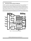

Serial Host Interface Programming Model
DSP56364 24-Bit Digital Signal Processor Users Manual, Rev. 2
Freescale Semiconductor 7-9
When in Master mode and CPHA = 1, the DSP core should write the next data word to HTX when
HTDE = 1, clearing HTDE. The HTX data will be transferred to the shift register for transmission as soon
as the shift register is empty. HTDE is set when the data is transferred from HTX to the shift register.
The clock phase and polarity should be identical for both the master and slave SPI devices. CPHA and
CPOL are functional only when the SHI operates in the SPI mode, and are ignored in the I
2
C mode. The
CPHA bit is set and the CPOL bit is cleared during hardware reset and software reset.
7.4.5.2 HCKR Prescaler Rate Select (HRS)—Bit 2
The HRS bit controls a prescaler in series with the clock generator divider. This bit is used to extend the
range of the divider when slower clock rates are desired. When HRS is set, the prescaler is bypassed. When
HRS is cleared, the fixed divide-by-eight prescaler is operational. HRS is ignored when the SHI operates
in the Slave mode, except for I
2
C when HCKFR is set. The HRS bit is cleared during hardware reset and
software reset.
NOTE
Use the equations in the SHI data sheet to determine the value of HRS for
the specific serial clock frequency required.
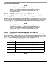
7.4.5.3 HCKR Divider Modulus Select (HDM[7:0])—Bits 10–3
The HDM[7:0] bits specify the divide ratio of the clock generator divider. A divide ratio between 1 and
256 (HDM[7:0] = 0 to $FF) may be selected. When the SHI operates in the Slave mode [except for I
2
C
when HCKFR is set], the HDM[7:0] bits are ignored. The HDM[7:0] bits are cleared during hardware reset
and software reset.
NOTE
Use the equations in the SHI data sheet to determine the value of HDM[7:0]
for the specific serial clock frequency required.
7.4.5.4 HCKR Reserved Bits—Bits 23–14, 11
These bits in HCKR are reserved and unused. They are read as 0s and should be written with 0s for future
compatibility.
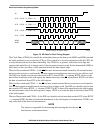
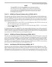
7.4.5.5 HCKR Filter Mode (HFM[1:0]) — Bits 13–12
The read/write control bits HFM[1:0] specify the operational mode of the noise reduction filters, as
described in Table 7-3. The filters are designed to eliminate undesired spikes that might occur on the clock
and data-in lines and allow the SHI to operate in noisy environments when required. One filter is located
in the input path of the SCK/SCL line and the other is located in the input path of the data line (i.e., the
SDA line when in I
2
C mode, the MISO line when in SPI Master mode, and the MOSI line when in SPI
Slave mode).