


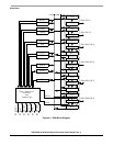

ESAI Data and Control Pins
DSP56364 24-Bit Digital Signal Processor Users Manual, Rev. 2
6-6 Freescale Semiconductor
SCKT may be programmed as a general-purpose I/O pin (PC3) when the ESAI SCKT function is not being
used.
NOTE
Although the external ESAI serial clock can be independent of and
asynchronous to the DSP system clock, the DSP clock frequency must be at
least three times the external ESAI serial clock frequency and each ESAI
serial clock phase must exceed the minimum of 1.5 DSP clock periods.
6.2.9 Frame Sync for Receiver (FSR)
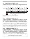
FSR is a bidirectional pin providing the receivers frame sync signal for the ESAI interface. The direction
of this pin is determined by the RFSD bit in RCR register. In the asynchronous mode (SYN=0), the FSR
pin operates as the frame sync input or output used by all the enabled receivers. In the synchronous mode
(SYN=1), it operates as either the serial flag 1 pin (TEBE=0), or as the transmitter external buffer enable
control (TEBE=1, RFSD=1). For further information on pin mode and definition, see Table 6-8 and on
receiver clock signals see Table 6-1.
When this pin is configured as serial flag pin, its direction is determined by the RFSD bit in the RCCR
register. When configured as the output flag OF1, this pin reflects the value of the OF1 bit in the SAICR
register, and the data in the OF1 bit shows up at the pin synchronized to the frame sync being used by the
transmitter and receiver sections. When configured as the input flag IF1, the data value at the pin is stored
in the IF1 bit in the SAISR register, synchronized by the frame sync in normal mode or the slot in network
mode.
FSR may be programmed as a general-purpose I/O pin (PC1) when the ESAI FSR function is not being
used.
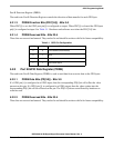
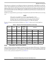
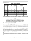
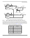
Table 6-2 Transmitter Clock Sources
THCKD TFSD TCKD
Transmitter
Bit Clock
Source
OUTPUTS
000SCKT
0 0 1 HCKT SCKT
010SCKT FST
0 1 1 HCKT FST SCKT
1 0 0 SCKT HCKT
1 0 1 INT HCKT SCKT
1 1 0 SCKT HCKT FST
1 1 1 INT HCKT FST SCKT