


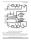

ESAI Programming Model
DSP56364 24-Bit Digital Signal Processor Users Manual, Rev. 2
Freescale Semiconductor 6-15
transmitter #4 is disabled after completing transmission of data currently in the ESAI transmit shift
register. Data can be written to TX4 when TE4 is cleared but the data is not transferred to the transmit shift
register #4.
The SDO4/SDI1 pin is the data input pin for RX1 if TE4 is cleared and RE1 in the RCR register is set. If
both RE1 and TE4 are cleared the transmitter and receiver are disabled, and the pin is tri-stated. Both RE1
and TE4 should not be set at the same time.
The normal mode transmit enable sequence is to write data to one or more transmit data registers before
setting TEx. The normal transmit disable sequence is to clear TEx, TIE and TEIE after TDE equals one.
In the network mode, the operation of clearing TE4 and setting it again disables the transmitter #4 after
completing transmission of the current data word until the beginning of the next frame. During that time
period, the SDO4/SDI1 pin remains in the high-impedance state. The on-demand mode transmit enable
sequence can be the same as the normal mode, or TE4 can be left enabled.
6.3.2.6 TCR ESAI Transmit 5 Enable (TE5) - Bit 5
TE5 enables the transfer of data from TX5 to the transmit shift register #5. When TE5 is set and a frame
sync is detected, the transmit #5 portion of the ESAI is enabled for that frame. When TE5 is cleared, the
transmitter #5 is disabled after completing transmission of data currently in the ESAI transmit shift
register. Data can be written to TX5 when TE5 is cleared but the data is not transferred to the transmit shift
register #5.
The SDO5/SDI0 pin is the data input pin for RX0 if TE5 is cleared and RE0 in the RCR register is set. If
both RE0 and TE5 are cleared the transmitter and receiver are disabled, and the pin is tri-stated. Both RE0
and TE5 should not be set at the same time.
The normal mode transmit enable sequence is to write data to one or more transmit data registers before
setting TEx. The normal transmit disable sequence is to clear TEx, TIE and TEIE after TDE equals one.
In the network mode, the operation of clearing TE5 and setting it again disables the transmitter #5 after
completing transmission of the current data word until the beginning of the next frame. During that time
period, the SDO5/SDI0 pin remains in the high-impedance state. The on-demand mode transmit enable
sequence can be the same as the normal mode, or TE5 can be left enabled.
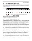
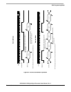
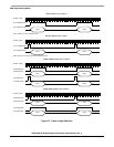
6.3.2.7 TCR Transmit Shift Direction (TSHFD) - Bit 6
The TSHFD bit causes the transmit shift registers to shift data out MSB first when TSHFD equals zero or
LSB first when TSHFD equals one (see Figure 6-13 and Figure 6-14).
6.3.2.8 TCR Transmit Word Alignment Control (TWA) - Bit 7
The Transmitter Word Alignment Control (TWA) bit defines the alignment of the data word in relation to
the slot. This is relevant for the cases where the word length is shorter than the slot length. If TWA is
cleared, the data word is left-aligned in the slot frame during transmission. If TWA is set, the data word is
right-aligned in the slot frame during transmission.