


Data and Program memory
DSP56364 24-Bit Digital Signal Processor Users Manual, Rev. 2
1-8 Freescale Semiconductor
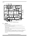
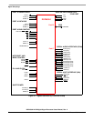
1.5.7 JTAG TAP and OnCE Module
The DSP56300 core provides a dedicated user-accessible TAP fully compatible with the IEEE 1149.1
Standard Test Access Port and Boundary Scan Architecture. Problems associated with testing high-density
circuit boards led to developing this standard under the sponsorship of the Test Technology Committee of
IEEE and JTAG. The DSP56300 core implementation supports circuit-board test strategies based on this
standard.
The test logic includes a TAP consisting of four dedicated signals, a 16-state controller, and three test data
registers. A boundary scan register links all device signals into a single shift register. The test logic,
implemented utilizing static logic design, is independent of the device system logic.
The OnCE module provides a nonintrusive means of interacting with the DSP56300 core and its
peripherals so a user can examine registers, memory, or on-chip peripherals. This facilitates hardware and
software development on the DSP56300 core processor. OnCE module functions are provided through the
JTAG TAP signals.
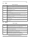
1.6 Data and Program memory
The on-chip memory configuration of the DSP56364 is affected by the state of the MS (Memory Switch)
control bit in the OMR register, and by the SC bit in the Status Register. Refer to Section 3, "Memory
Configuration".
1.6.1 Reserved Memory Spaces
The reserved memory spaces should not be accessed by the user. They are reserved for future expansion.
1.6.2 Program ROM Area Reserved for Freescale Use
The last 128 words ($FF2F80-$FF2FFF) of the Program ROM are reserved for Freescale use. This
memory area is reserved for use as expansion area for the bootstrap ROM as well as for testing purposes.
Customer code should not use this area. The contents of this Program ROM segment is defined by the
Bootstrap ROM source code in Appendix A, "Bootstrap ROM".
1.6.3 Bootstrap ROM
The 192-word Bootstrap ROM occupies locations $FF0000-$FF00BF. The bootstrap ROM is
factory-programmed to perform the bootstrap operation following hardware reset. The contents of the
Bootstrap ROM are defined by the Bootstrap ROM source code in Appendix A, "Bootstrap ROM".
1.6.4 Dynamic Memory Configuration Switching
The internal memory configuration is altered by re-mapping RAM modules from Y data memory into
program memory space and vice-versa. The contents of the switched RAM modules are preserved.
The memory can be dynamically switched from one configuration to another by changing the MS bit in
OMR. The address ranges that are directly affected by the switch operation are specified in Table 3-1 The