


SHI Programming Considerations
DSP56364 24-Bit Digital Signal Processor Users Manual, Rev. 2
7-20 Freescale Semiconductor
7.7 SHI Programming Considerations
The SHI implements both SPI and I
2
C bus protocols and can be programmed to operate as a slave device
or a single-master device. Once the operating mode is selected, the SHI may communicate with an external
device by receiving and/or transmitting data. Before changing the SHI operational mode, an SHI
individual reset should be generated by clearing the HEN bit. The following paragraphs describe
programming considerations for each operational mode.
7.7.1 SPI Slave Mode
The SPI Slave mode is entered by enabling the SHI (HEN = 1), selecting the SPI mode (HI
2
C = 0), and
selecting the Slave mode of operation (HMST = 0). The programmer should verify that the CPHA and
CPOL bits (in the HCKR) correspond to the external host clock phase and polarity. Other HCKR bits are
ignored. When configured in the SPI Slave mode, the SHI external pins operate as follows:
• SCK/SCL is the SCK serial clock input.
• MISO/SDA is the MISO serial data output.
• MOSI/HA0 is the MOSI serial data input.
•SS/HA2 is the SS Slave Select input.
•HREQ is the Host Request output.
In the SPI Slave mode, a receive, transmit, or full-duplex data transfer may be performed. Actually, the
interface simultaneously performs both data receive and transmit. The status bits of both receive and
transmit paths are active; however, the programmer may disable undesired interrupts and ignore
non-relevant status bits. It is recommended that an SHI individual reset (HEN cleared) be generated before
beginning data reception in order to reset the HRX FIFO to its initial (empty) state (e.g., when switching
from transmit to receive data).
If a write to HTX occurs, its contents are transferred to IOSR between data word transfers. The IOSR data
is shifted out (via MISO) and received data is shifted in (via MOSI). The DSP may write HTX using either
DSP instructions or DMA transfers if the HTDE status bit is set. If no writes to HTX occurred, the contents
of HTX are not transferred to IOSR, so the data that is shifted out when receiving is the same as the data
present in the IOSR at the time. The HRX FIFO contains valid receive data, which may be read by the DSP
using either DSP instructions or DMA transfers, if the HRNE status bit is set.
The HREQ
output pin, if enabled for receive (HRQE1–HRQE0 = 01), is asserted when the IOSR is ready
for receive and the HRX FIFO is not full; this operation guarantees that the next received data word will
be stored in the FIFO. The HREQ output pin, if enabled for transmit (HRQE1–HRQE0 = 10), is asserted
when the IOSR is loaded from HTX with a new data word to transfer. If HREQ is enabled for both transmit
and receive (HRQE1–HRQE0 = 11), it is asserted when the receive and transmit conditions are true
simultaneously. HREQ is deasserted at the first clock pulse of the next data word transfer. The HREQ line
may be used to interrupt the external master device. Connecting the HREQ line between two SHI-equipped
DSPs, one operating as an SPI master device and the other as an SPI slave device, enables full hardware
handshaking if operating with CPHA = 1.
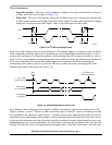
The SS
line should be kept asserted during a data word transfer. If the SS line is deasserted before the end
of the data word transfer, the transfer is aborted and the received data word is lost.