


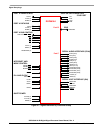

Interrupt and Mode Control
DSP56364 24-Bit Digital Signal Processor Users Manual, Rev. 2
2-6 Freescale Semiconductor
2.6 Interrupt and Mode Control
The interrupt and mode control signals select the chip’s operating mode as it comes out of hardware reset.
After RESET
is deasserted, these inputs are hardware interrupt request lines.
RD Output Tri-stated Read Enable—RD is an active-low output that is asserted to read external
memory on the data bus. This signal is tri-stated during hardware reset and when
the DSP is in the stop or wait low-power standby mode.
WR Output Tri-stated Write Enable— WR
is an active-low output that is asserted to write external
memory on the data bus. This signal is tri-stated during hardware reset and when
the DSP is in the stop or wait low-power standby mode.
TA Input Ignored Input Transfer Acknowledge—If there is no external bus activity, the TA
input is
ignored. The TA
input is a data transfer acknowledge (DTACK) function that can
extend an external bus cycle indefinitely. Any number of wait states
(1, 2. . .infinity) may be added to the wait states inserted by the BCR by keeping
TA
deasserted. In typical operation, TA is deasserted at the start of a bus cycle,
is asserted to enable completion of the bus cycle, and is deasserted before the
next bus cycle. The current bus cycle completes one clock period after TA
is
asserted synchronous to the internal system clock. The number of wait states is
determined by the TA
input or by the bus control register (BCR), whichever is
longer. The BCR can be used to set the minimum number of wait states in
external bus cycles.
In order to use the TA
functionality, the BCR must be programmed to at least one
wait state. A zero wait state access cannot be extended by TA
deassertion,
otherwise improper operation may result. TA
can operate synchronously or
asynchronously, depending on the setting of the TAS bit in the operating mode
register (OMR).
TA
functionality may not be used while performing DRAM type accesses,
otherwise improper operation may result.
Table 2-7 External Bus Control Signals (continued)
Signal
Name
Signal
Type
State during
Reset
Signal Description