


Intel
®
IXP400 Software
Access-Layer Components: HSS-Access (IxHssAcc) API
Programmer’s Guide IXP400 Software Version 2.0 April 2005
Document Number: 252539, Revision: 007 193
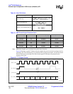
The HSS coprocessor communicates with an external device using three signals per direction: a
frame pulse, clock, and data bit. The data stream consists of frames — the number of frames per
second depending on the protocol. Each frame is composed of time slots. Each time slot consists of
8 bits (1 byte) which contains the data and an indicator of the time slot’s location within the frame.
The maximum frame size is 1,024 bits and the maximum frame pulse offset is 1,023 bit. The line
clock speed can be set using the API to one of the following values to support various E1, T1 or
aggregated serial (MVIP) specifications:
The frame size and frame offsets are all programmable according to differing protocols. Other
programmable options include signal polarities, signal levels, clock edge, endianness, and choice
of input/output frame signal.
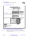
HSS Output Clock Jitter and Error Characterization
The high-speed serial (HSS) port on the processors can be configured to generate an output clock
on the HSS_TXCLK pin. This output clock, however, is not as accurate as using an external
oscillator. If the system is intended to clock a framer, DAA, or other device with a sensitive input
PLL, an external clock should be used.
Clock signalling is defined in the file IxHssAccCommon.c. The following tables describe the error
and jitter characteristics of signals based upon the values established in the IXP400 software.
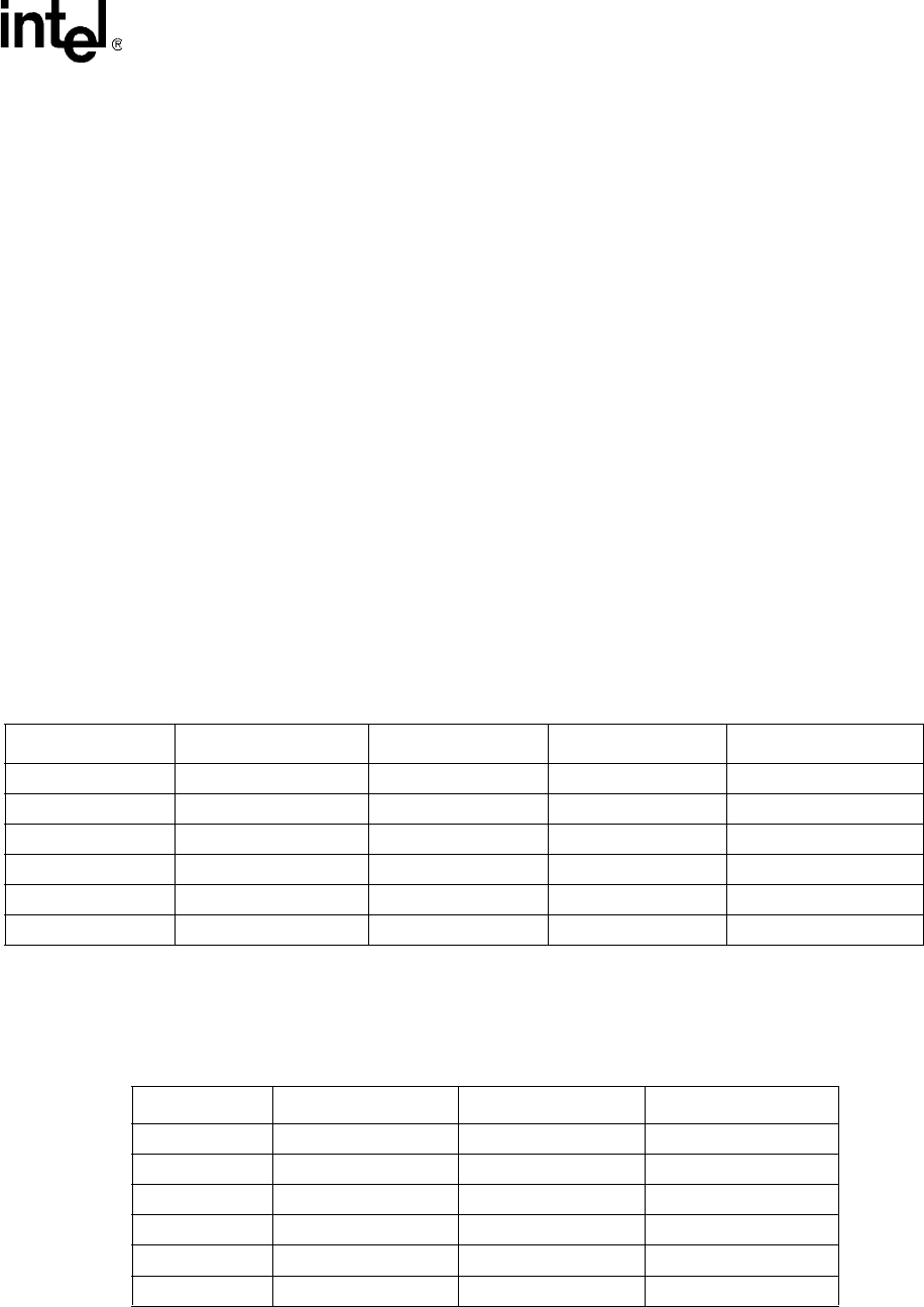
Note: Characterization data of the HSS TX clock output frequency data was determined by silicon
simulation. PPM parts per million error rate is calculated using average output frequency vs. ideal
frequency.
• 512 KHz • 1.536 MHz • 1.544 MHz
• 2.048 MHz • 4.096 MHz • 8.192 MHz
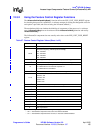
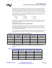
Table 38. HSS Tx Clock Output frequencies and PPM Error
HSS Tx Freq. Min. Freq. (Mhz) Avg. Freq. (Mhz) Max. Freq. (Mhz) Avg. Freq. Error (PPM)
512 KHz 0.508855 0.512031 0.512769 -60.0096
1.536 MHz 1.515 1.536 1.55023 -60.0096
1.544 MHz 1.515 1.5439 1.55023 +60.0024
2.048 MHz 2.01998 2.0481 2.08313 -60.0096
4.096 MHz 3.92118 4.0962 4.16625 -60.0096
8.192 MHz 7.4066667 8.1925 8.3325 -60.0096
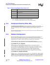
Table 39. HSS TX Clock Output Frequencies and Associated Jitter Characterization
HSS Tx Freq. Pj Max (ns) Cj Max (ns) Aj Max (ns)
512 KHz 12.189 15 18.283
1.536 MHz 9.063 15 86.102
1.544 MHz 12.359 15 210.099
2.048 MHz -8.204 15 118.957
4.096 MHz 10.9 15 190.742
8.192 MHz 12.951 15 226.634