Theory of
Operation
-
494A/494Ap
Servtce,
Vot.
1
Fllter
to
Mlxer
RF
Input
Cable.
Several
products
and harmonics
of
the
local
oscillator
and
RF input
fre-
quencies
will
exit
the
mixer
via
the
RF
input
port
of
th€
mixer.
The
image
(RF
input
minus
the
2nd
LO)
and
the
sum
(RF
input
plus
the
2nd
LO)
are
two
significant pro_
ducts.
There is enough
energy
in
these
two
signals
to
warrant
efforts
to
r€cover
that
energy.
Onfy
the RF signal
at
2072
MHz
can
pass
through
the four-cavity
filter.
Thus,
any
other
signal
frequeniy
that
is
applied
to
th€ filter
(that
is, signils
exiting
thi
mixer
via
the RF
port)
is
reflected
back
to
the
mixlr
by
the
filter.
lf
the
cable
betweEn
the filter
and
the mixer
is
the
correct
length, the
most
slgnificant
reflected
signals
(i.e.,
the
image
and
th€
sum)
can
be returned
to the
mixer
in
phase
and
convert€d
into
additional
€nergy
at
the
intermediate
frequency.
This
technique
is called
"image
enhancement
mixing,,
and
typically
improves
conversion
loss by approximately
3 dB
at
the
design
frequencies.
The
image frequency,
in
this
instance,
is very
near
the RF frequency.
A very
sharp
cut-off
filter
is
required
to
pass
the RF,
yet
refl€ct
the image.
The four_cavity
filter
performs
this
function.
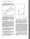
2nd
LO
lo Mlxer
LO Input
Cable.
The
image
and
sum
products
are also
present
at
the LO
port
of
the
mixer.
These
signals
leave
the
mixer
via
the cable
to
the 2nd
LO and are reflectEd
back
to
the mixer
by
the
LO .The oscillators
resonator
appears
highly
reflective
to
the
image
and sum
signals
because
it is
tuned
to the
LO
frequency.
Again,
the
length
of
the
cable
from
the
LO
to th€ mixer LO
port
is adjusted
so
the lmage
and
sum signals
are rEflected
back
to
the mixer,
in
the
proper
phase,
for
re-conversion
to suppty
additional
energy
at
the lF frequency.
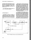
2182
MHz PHASE
LOCKED
2nd
LO
(Diagrams
13
and
i4)
The
2182
MHz
phase
locked
2nd
LO assembly
con_
tains
a tunable
microwave
oscillator,
frequency
refer_
ence,
and
phase
lock circuitry.
A
two-section
housing
contains
the
circuitry.
Microwave
circuitry
is
packaged
within
the
machined aluminum portion
of
the housing.
Low
frequency
phase
lock
circuitry
is
within
the mu-
metal
compartment,
In
the
microwave
or
LO
portion
of
the assembly,
the
2182 MHz
Microstrip
Osciilator
g€nerates
2Ig2
MHz tor
the
2nd converters
and
the 2nd
LO
internal
reference
circuitry.
The
2200 MHz
Reference
circuit
receives
a
100 MHz
drive
signal
from
the
grd
convert€r
crystal
oscillator
and
produces
100
MHz
harmonics.
The
i2nd
harmonic
or 2200
MHz
is
mixed
with
21g2MHz
from
the microstrip
oscillator
in
the
2Z0O
MHz
Reference
7-10
Mixer
circuit.
The
difference frequency
of
18 MHz
is
then
fed
to the
phase
lock
side of
the
module.
A
phase/frequency
detector, on
the
16-20
MHz
Phase
Lock
circuit
board, compares
the 18
MHz
difference
frequency
with
a signal from
a linearized
varactor
tuned, 18MHz
voltage controlled oscillator.
The
det€ctor output
tunes
the 2182 MHz
Microstrip
Oscillator such
that the
difference
frequency
exactly
matches
the
frequency
of
the
18
MHz
reference
VCO.
Sweep
and
tune signals
from
the Span
Attenuator
and
Cent€r Frequency
Control circuits tune
the
18
MHz
VCO. The
output
voltage
from
the
phase/frequency
detector forces
the
Microstrip
Oscillator to tune
the
same amount.
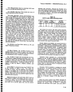
2182 MHz
Microstrip
Osciltator
(Diagram
14)
This
oscillator
consists
of a
printed
1/2 wavelength
resonator
driven
by
a
common-emitt€r feedback
amplifier
(01021).
The
base
of
Q1021
is capacitivety
tapped into
the
resonator.
The resonator
serves
as a
tuned
phase
inv€rter and
impedance
transformer, con-
nected
between
the
base
and coll€ctor of
Q1021
.
Part
ot
the
base feedback capacitance
is
provided
by a
bendable
tab
(C'1021).
This
allows line
adjustment
of
the total feedback.
This feedback
RF
signal
is
detected,
by
the base-
emitter
junction
of
Q1021,
to
produce
a change
in
bias
voltage
that
is
related
to the
amount
of feedback.
The
base voltage can
be moni-
tored at
TP1015 with
a high impedance voltmeter
without
significantly
disturbing the oscillator.
The
dc
collector
voltage
and current
for
Q1 021 is
regulated
by an activ€ feedback
circuit
containing
transistor
Q2021. Voltage at
the
junction
of
R2023 and
L2023
is a
function of
Ql021
collector
current.
This
vol-
tage
is
sensed
by Q2021,
which
alters the base current
to
Q1 021 thereby regulating
the
collector current and
maintaining
+10 Vdc on
the resonator. Decoupling and
control
of
bias
loop
dynamics are
provided
by C2104.
Resistor
R201 6
swamps
the
negative
base
resistance
of
Q102'l to
provide
stabilization.
Resistor
R2015
pro-
tects th€
base-
emitter
junction
of
Q1021
trom exc€s-
sive reverse
bias in
the
event
the
+12
V
supply fails.
The
oscillator
is
tuned
by
varactor
diode CR1028,
connected
to
one end of
the
resonator. Decoupling
for
the
varactor
is
provided
by
the
low-pass elements
in
the
tune
fine. Bendable
tab C1022 can be used to
fine tune
the
oscillator center
frequency.
Three
output taps are coupled
to
the
resonator
through
printed
capacitors
under
the
resonator.
One
output
supplies 2182 MHz
through
a
6
dB
attenuator
to
the
Harmonic Mixer
in the 829
MHz
2nd
Converter.
The
other
two
output
taps
coupl€
LO
power
through
6
dB
attenuators
to buffer
amplifiers
Ql031
and Ql0'll.
The
o
o
o
o
o
o
O
a
o
o
o
a
o
o
o
o
O
o
o
o
a
o
O
o
o
o
a
o
o
O
a
a
o
o
o
o
O
o
o
o
o
o
o
o


