Theory
of
Operation
-
4g4[l494fup
Servlce,
Vol.
1
drifts
negative,
the other
half of
UlO.l5 conducts,
caus_
ing
reverse
action
to
occur.
-
Normally,
the
input
signal
to
the
window
comparator
is attenuat€d
by
R2040,
which
reduces
the
voltage
applied
to
U101S
to
0.9%
of
the output
from
U204-g.
This allows
U2048
to
drift
up
and down
without
immedi-
ately
triggering
either
comparator.
when
R2043
is
in
the
circuit,
it is
called
,'wide
window,'operation.
When
phase
lock
is
de-selected,
the
microcomputer
selects
narrow
window
(which
bypasses
R2049).
The
Center
Frequency
Controt
circuit
is
then instiucted
by
the
microcomputer
to
move
the
1st
LO frequency
uniit
tne
window
comparator
indicates
that the FM
coil
current
is
near
zero.
This
prevents
the lst LO
frequency
from
shifting
too far from
the
lock
point
when
phase
lock
is
canceled.
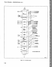
The F
ERROR
signal
is
used
by
the
Counter
board
(A51)
for
diagnostics
so
that
the
microcomputer
can
determine
the
relationship
between
.t
st LO
irequency
and
the strob€
line.
The
F
ERROR
signal
is
generatei
from
thE
outer
loop
ERROR
signal
from
the
phase
Gate
Detector (A24).
The
circuit
consists
of
an
active
low-
pass
filter
U2065
and
Schmitt
trigger
U1Og5.
This cir-
cuit
ftlters
and
squares
the incoming
ERROR
signal.
The ERROR
signat
is
apptied
through
CZO67
to
an
nC
500 kHz
low-pass
filter
and
amptifier
U2O6S.
After
fitter-
ing,
the signal
is applied
through
Enor
Count
Break_
point
adjustment
Rl061
to
the input of
u1035,
a
schmitt
trigger circuit.
The
squared
output
signal
is
then
applied
to circuits
on
the
Counter
board.
The
STROBE
ENABLE
signat
enabtes
the strobe
generator
in
the
Strobe Driver
circuit
(ASOA2).
Shift
register
U2025
reads
the instrument
bus latch
on
the
counter
board
(A51)
to
determine
the status
of
the
STROBE
ENABLE
signat.
O20gO
inverts
the signat
and
converts
it
to TTL
level
to drive
the
strobe
generator.
controlted
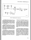
oscillator
(vcol.
The controiled
oscilla-
tor
(VCO)
is
a
voltage-controlled
crystal
oscillator
whose
frequency
is
controlled
by
the
output
of
the Error
Ampllfier. The
oscillator generates
a
reference
signal
that as
used
to stabilize
the lst
LO frequency.
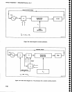
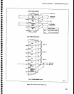
Refel
to
the block
diagram
adjacent
to
Diagram
40
for a
func_
tional
description
of
this
part.
The
control
voltage
from
the
Error Amplifier,
which
is
a function
of
th€
difierence
between
the
microcom-
puter
controlled
+N
signal
and
the
Offset
Mixer
difference
frequency,
is applied
to the
VCO
on
the
Con-
trolled
Oscillator
board
to regulate
its
frequency
of
operation.
The circuit
has
two outputs:
the first,
which
is
part
of
the
inner
loop
of
the
phase
lock
circuits,
is
fed
to the
Offset
Mixer,
where
it is
used to
derive
the
difference
frequency
that is
compared
against
the
+N
signal.
The
second
output,
which
is
part
of
the outer
loop,
is
led
to
the Strobe
Driver
circuits.
where
it is
7-86
divided
down to becomE
th€
STROBE
signal
that is
compared
against
the l st
LO signal
in
the
phase
Gate.
The
VCO consists
of five
major
circuits,
four
of
which
are
connected in
a
positive
feedback
loop
to sus-
tain oscillation.
These circuits
ar€
the resonator
stage,
the
differential
amplifier,
the
bandpass
lilter,
the isola-
tion amplifier,
and
the
output
amplifier.
The
resonator
stage operates
at
a
frequency ot
2S.OS2MHZ
to
25.094
MHz.
Th€ output
signal
from
the resonator
is
applied
to
the
input of
a
differential
amplifier
which
drives
the output amplifier
and
the
bandpass
filter.
The
output
from
the
output
amplifier
is
fed
to
the
Offset
Mixer
and
the
Strobe
Driver.
The
bandpass
filter
strips
the signal of any
spurii €ither
side of csnter
frequency
and
feeds
th€ signal
to the isolation
amplifier.
This
stage
furnishes
the
positive
feedback
drive
to the
reso-
nator stage and
isolates the bandpass
filter from
the
resonator
stage.
The
resonator stage
consists
of
crystal
y1012,
varactor
diodes
CR1011
ancl
CRl012,
and r€lated
com-
ponents.
The stage operates
within
the
frequency
range of
25.032
MHz
to
25.094
MHz,
which is
controil€d
by
the voltage applied
to
varactor
diodes
CR1011
and
cRl0l2.
Feedback energy
for sustaining
oscillations
comes from
the
isolation
amplifier
by way of coil
Ll025.
The
resonator output
signal
is applied
to a
differential
amplifier
Q2033
and
Q2041. The
Q2033
side
drives
the output amplifier and serves
to
isolate
the out-
put
load from
the feedback
loop.
Gain from
this side is
less
than one. The signal
is fed
from
the collector
of
Q2041, following
amplification,
to
the band-pass filter.
The band-pass filter
consists of
passive
com-
ponents,
and
is used
to
strip
the
signal
of any frequency
components
more
than
about
40
kHz away from
the
center
operating
frequency, which is
approximately
25.06
MHz.
Capacitors C1041 and
C1042 ar€ adjusted
at
th€
factory
to
set
the bandwidth and cent€r
the
fre-
quency
of
the filter.
The
isolation amptifier,
01028, is a common-base
configuration,
in order to match
the
impedance
of
the
filter
to the resonator.
Output
current
from the stage
furnishes
positive
feedback for
the
resonator.
The
output
amplifier. consisting of
transistors Q2025
and
Q2026, is connected as
a differential amplifier with
02026 driving
one
side
of
the Offset
Mixer and
Q2025
driving
the input
of
the
Strobe Driver circuit, for
eventual
application
to the
Phase
Gate
circuits.
Strobe
Drlver
Clrcult. The Strobe Driver circuit
con-
sists
of counter
U1022,
bandpass filter FL2064, sourc€
follower
02091
,
and AND
gates
U1091A
and
U10918.
o
I
o
o
o
o
o
a
o
I
o
o
o
a
o
o
o
e
o
o
a
o
o
o
o
o
o
o
o
o
t
o
o
o
o
I
O
o
o
o
o
o
o
o


