Theory
of
Operaton
-
4g4A/4g4Ap
Servtce,
Vol.
1
o
The
tracking
adjustment
circuit,
which
compensates
for
different
preselector
sensitivities,
compensat€s
any
pres€lector
offset,
and
compensates
for
non-
linear operation
caused
by
magnetic
saturation
of
the Preselector.
r
The final
driver stage,
which
changes
the
applied
signal
voltage
into
a
current
drive for
the
preselec-
tor coil.
e
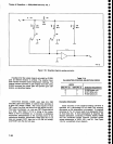
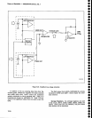
The
preselector
switch
driver,
which
drives
the filter
sElect
switch€s,
shown
on
Diagram
12.
The
switches
require
a
positive
putse
to select
the
Low-pass
Filter
and
a n€gativg
pulse
to
select
the
PresElector.
Digital
Control
Circuits
The
microcomputer
interface
circuits,
which exer-
cis€
digital
control
of
the
preselector
Driver
circuits,
consist of address
decoder
US0g6 and latch
U5O3l.
Both the write
address
(27)
and
the
read address (F7)
are decoded
by
U5036.
Data
is latched
into
u5031
on
the trailing
edge
of
the
DATA
VALID
signal
for
address
77.
This
event
coincides
with
the rising
edge
of
th€
pulse
on
pin
3
of
U5036.
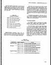
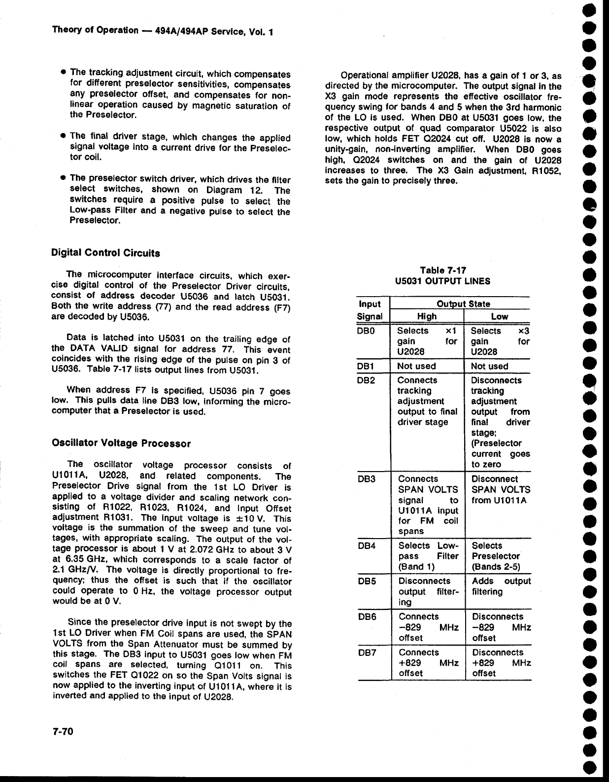
Table
7-17
tists
output
tines
from
U5Og1.
When address
F7
is
specified,
US0g6
pin
7
goes
low.
This
pulls
data line
DB3 low,
informing
the micro-
computer
that a
Preselector
is
used.
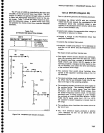
Oscillator Voltage
Processor
The
oscillator
voltage
processor
consists
of
Ul011A,
U2028,
and
retated
components.
The
Preselector
Drive
signal
from
the
1st LO Driver
is
applied
to
a
voltage
divider and
scaling
network
con-
sisting of
Rl022,
Rl023.
R1024,
and lnput
Offset
adjustment
R1031.
The input
vottage
is *10V.
This
voltage is
the summation
of
the sweep and
tune vol-
tages,
with
appropriate
scaling.
The output
of
the vol-
tage
processor
is about
1 V at
2.A72
GHz to
about
g
V
at 6-35
GHz, which
corresponds
to
a scale
factor
of
2.1 GHz/V. The
voltage
is
directly
proportional
to
fre-
quency;
thus
the
offset
is
such
that
if
the oscillator
could
operate
to
0 Hz,
the voltage
processor
output
would
be
at
0 V.
Since the
preselector
drive
input
is not
swept
by the
1st LO Driver
when
FM
Coil spans
are
used,
tfre
SpnN
VOLTS from
the
Span
Attenuator
must
be
summed
by
this
stage.
The
DB3
input
to
u5031
goes
low
when
FM
coil
spans
are selected,
turning
0101 1 on.
This
switches the FET
01022
on so
the
Span
Volts
signal is
now
applied
to
the inverting
input
of
U1011A, where it is
inverted and applied
to the
input
ol lJ21Zg.
7,70
Operational
amplifier
U2028,
has
a
gain
of 1
or
3, as
directed by
the
microcomputer.
The output
signal in
the
X3
gain
mode
represents
the
effective
oscillator
fre-
quency
swing
for
bands
4 and
5
when
the 3rd harmonic
of
the
LO is
used.
When
DBo at
U5031
goes
tow,
the
respective output of
quad
comparator
u5022
is
also
low,
which holds
FET
c.2024 cut ofi.
V2028 is
now a
unity-gain, non-inverting amplifier.
When
DBO
goes
high,
O2024
switches
on and
the
gain
of
U2028
increases
to
three.
The X3
Gain adjustment,
R1052,
sets
the
gain
to
precisely
three.
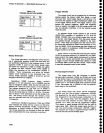
Table 7-17
U5031 OUTPUT LINES
o
O
o
o
e
o
o
I
o
o
I
e
o
o
o
a
o
a
o
a
o
a
o
o
o
o
o
a
o
O
I
I
o
o
o
o
a
o
o
o
o
o
I
o
Input
liqnal
High
Low
DBO
Selects
x1
gain
for
u2028
Selects
gain
u2028
x3
for
DB1
Not
used Not
used
DB2 Gonnects
tracking
adjustment
output
to
final
driver
stage
Disconnects
tracking
adjustment
output
from
final
driver
stage;
(Preselector
currerit
goes
to
zero
DB3 Connects
SPAN
VOLTS
signal
to
Ul011A
input
for FM coil
spans
Disconnect
SPAN
VOLTS
from
Ul011A
D84 Selects
pass
(Band
1)
Low-
Filter
Selects
Preselector
(Bands
2-5)
DB5
Disconnects
output
filter-
ing
Adds output
filtering
DB6 Connects
-829
MHz
off set
Disconnects
-829
MHz
offset
DB7
Connects
+829 MHz
offset
Disconnects
+829
MHz
offset


