


t
o
)
o
t
t
I
o
o
o
o
o
I
I
a
o
o
I
o
I
o
o
o
a
o
o
I
o
I
t
o
o
o
o
o
o
I
D
o
o
o
a
t
o
stored
in
the
display
shift
register.
Then,
as
th€
A
value
is- read.
it
is cornpared
with
the
B
value
and
the larger
of
the two is
loaded
into
the
disptay
shift
regisier.
Finally,
the
number
in
the
shift
registei
is
writte;
into
memory._
This
operation
is
performed
once
each
time
that
th€
save
A
mode
is
selected.
Vertical
control
lC
U2090
contains
a
3-bit synchro_
nous
counter
that id€ntifies
the
specific
bit of
in
g,bit
vertical
value
that
is
to
be read
from
memory
or
written
into
memory.
This
is
the
only
memory
addressing
that
is
performed
by
U2030.
All other
addrdssing
is
performed
!y
tne horizontat
control
lC
(on
the
Hoiizontat
Digital
Storage
board).
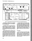
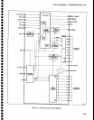
Dlgltzlng
Clrcults.
The
input
vertical
signat,
VtD
FLTR
OUT, coupled
through
edge
connector pin
60
is
applied
through
buffer
U3040
to
sampte
and hoid
switch
U2040C.
U2040C
is
controiled
by frip-flop
U10108.
U10108
generates
the
sample puise,
and
is
enabled
9uljng
the
ctock
cycte
after
tne
iast
approximation,
as
indicated
by
the
least
significant
bit trom
the
successive
approximation
register
in
U2030.
The
switched
sample
is
then applied
through
buffer
U1045
to a
summing
junc_
tion. At
this
point
the
output
current
from
Oigitifto-
analog
converter
Ug02S,
that is
supplied
from
the suc_
cessive
approximation
register
in
Ui03O,
is
subtracted
from
the sample
current.
The
difference
current
is
then
fpRlieO
thr-o-ugh comparator
U2O3SB
and synchronizing
flip-flop,
y:2027A,
to
pin
18
of
U2030
as
th;
UpiDowti
slOnal.
The
binary
equivatent
of
the input
sample
is
sfiectively
produced
by
the
combination
of
the succes-
sive
approximation
register,
the
digital_to-analog
con_
verter,
and
the
sample
and
hold
circuit.
Address
Decoding.
The
address
decode
logic
accepts
inputs
from
the
address
bus
and trom
the
address
control
logic
on
the
Horizontal
Digital
Storage
board,
producing
the
control
signals
for
read
and
wri-te
operations:
CONT W
(control
write)
DATA
W
(data
write)
DATA R
(data
read)
The
control
write
signal gates
the
control
word
from
the
data bus
into
control
register
UZOZ'
to
generate
mode
control
signals.
This
control
word
consists
of one
bit, 04,
that
represents
the front-panel
MAX
HOLD
func-
tion.
lf output
Q5 is
low,
a
peak
operation
is
forced;
if
output
Q5
is
high
and
e6 is low,
an
average
operation
is
forced.
The
data
read
and
data
write
signals
are
applied
to the
interface
logic
to
control
memory
read
and
write
operations.
Theory
of
Operatlon
-
494A/4g4Ap
Servlce,
Vol. I
Interface
Logic.
The interface
logic,
in
general,
per-
forms
control and
interface
functions
between
the
active
data
circuits in
the vertical
and
horizontal
sections
and
the rest
of
the
instrument.
lt allows
the
microcomputer
to control
the storage
system
functions
and
to access
the
digital
storage
memory.
lt also
contains
th€
circuitry
for
serial-to-parallel
and
parallel-to-serial
conv€rsion.
(l'he
microcomputer
uses
parallel
transfer;
the
digital
:lollSe
memory
uses seriat
transfer.)
Shift regaster
U4020
reads
data
from
memory
to
the data
bus.
Regis-
ter U2025 stores
information
from
the
data bus
for
transfer
to
memory.
Multiplexer
U40i
5 does
the
parallel-to-serial
conversion
and
applies
the
data
output
to
gate
U30248, which
acts
as a
buffer
to
supply
eitirer
the multiplexer
output
or
the MEM
OUT
(memory
out_
put)
signal
from
U2030
to
the memory
as
the DSDa
(digi-
tal storagE
data Input)
data
train.
The interface
circuit group
on
the
Vertical
Digital
Storage
board is
the handshake
togic
that works
with
the horizontal
control
circuits
to access
th€
mernory and
to determine
when
to increment
the memory
address
counter.
In
either
a
data
read
or
data
write operation
(when
th€
corresponding
signal
goes
high),
flip-flop
U30208
is
triggered. This
reteases
the
BUS REe
(bus
request)
line
to allow
that signal
to
go
high
and signats
the horizontal
control
circuit
that memory
access
is
required.
When
th€ horizontal
circuits
recognize
the
request.
thos€
circuits
pull
the BUS
REO
line low
at
the
same
time
that SYNC is low.
The interface
logic
detects
the BUS
REQ
and
SYNC low
condition
through
U201SA,
U20158,
U3010A, and
U3015A,
and
produces
the tow
BUS
GRANT signal
to
indicate
memory
access.
The
BUS
GRANT signal
then enables
shift
register
U4020
to
shift
data from
memory
or enable
register
Ul02l
. BUS
GRANT also enables
multipl€xer
U401S
to
Ehlft
data
to
memory
as indicated
by the DATA
R and
DATA W tines.
At
the
end of
a
data read cycle, gates
U2010B and
U4030C
produce
the INCR
ADRS (increment
address)
signal
to
increment
the
address
register
in
the
horizon-
tal circuits.
Maximum Hold.
As
described
previously,
when
the
Max
Hold
mode
is
selected,
the signal
from
e4
of
con-
trof
register
V2428
causes
th€ circuits
in
Ul023
to
com-
pare
the binary
equivalent
of
th€ input
signal for
a
giv€n
X value
with
the
information
in
memory
for
that
same
X
value.
This
causes
the
larger
value
of
the two to be
stored
in
memory. The signal
from
04, in combination
with
the VALID signal from
the horizontal
circuits,
pro-
duces
the MAX HOLD command
to
U2090 through
inverter
U4030E
and
gate
U4040A.
Constant Circuit
As
described previously,
in
the
B
minus A
operation,
a
constant
is
used. This
constant is
selected
internally with
switch
3101
5, This switch,
in
7-43