


o
a
o
I
o
I
t
t
o
o
I
t
o
o
o
o
o
t
o
a
o
o
o
O
a
o
o
o
t
a
o
a
t
o
a
o
I
o
a
o
o
a
o
o
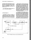
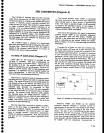
Because
the
grd
harmonic
of
719
MHz
is
locked
to
the 2182MHz
reference,
the
tuning
range
ot
tne
719
MHz
osciilator
is
onty
one
third
oithe
tuning
range
of
the reference.
Since.th:
rgnge
is
4
MHz,
ttre
ringe-ot
the
719
MHz
osciilator
is 71g
Jt.gg
trlnz.
'
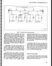
The
719
MHz
VCO
(O20i4)
uses
a
Cotpitts
configuration,
with
a
printed
circuit quarter-wavelength
transmission
line
resonator,
to
achieve
high
specir"t
purity
and
good
thermat
stability.
Correction
voliage
is
applied
to varactor
ctiode
CRldlt
(which
is
connected
at
the
midpoint
of
the
transmission
line
resonator)
to
vary
ths r€sonant
frequency
of
the
transmission
jine
ov€r a
1.5
MHz
range.
A
tunable
transmission
line
(atso
printed)
adjacent
to
the
printed
resonator
compensates
for
variations
in
component
tolerances
and
resonator
dimensions-
This
adjustable
transmission
line
is
cut,
at
factory
calibration,
to
the
correct
length
for
proper
VGO
operation.
A
scale
with
minor
divisions
every
iMHz
is
printed
next
to
th€
adjustabre
line
to aid
in
caribration.
The
output
from
the oscillator
is
extract€d
near
one
end
of
the
quarter-wavelength
line
through
two
printed
inductors
and
applied
to
output
amplitiers
through
a
power
splitter.
The
719MHz
VCO
is
enabted
or
disabted,
under
microprocessor
control,
dependent
upon
the
frequency
band.
being anatyzed,
by
the
tF
SELECT
line.
When
this
lin€
is
low,
e201 7
is
cut
off,
which
turns
e201
6 otr.
This,
in
turn,
cuts
off
transistor
e8015 (which
is
the
current
source
for oscillator
transistor
e20t+;,
tnus
disabling
the
719
MHz
oscillator.
From
the oscillator,
the
*6
dBm
719
MHz
output
signal
is
applied,
throu-gh
a
power
divider
consisting
of
resistors
Rl021,
Rl022,
and
Rl02O,
to
tsolation
amplifier
Q1021.
From
the
other
side
of
this
power
9iut9gr,
the signat
is
apptied
to
an
output
amptifier
(02021)
for
transmission
to
the
929 MHz
2nd
Converter
Mixer
circuit.
A
second
isolation
amplifier
(OgO21),
Il.e^n!i911
in
configuration,
provides
isotation
between
the
719
MHz
oscillator
output
and
any
undesired
Harmonic
Mixer
products.
The
829 MHz
Harmonic
Mixer
produces
not
only
the
required
25MHz
difference
frequency,
but also
many
higher
order
intermodulation
proOucts.
Two
of
these
frequencies,
744
MHz
and
6g4
MHz,
are
25
MHz
from
the 719
MHz
oscillator
frequency.
The
isolation
amplifiers,
01021
and
e3021,
provid6
sufficient
attenua_
tion in
the reverse
direction
to
prevent
these
products
from
getting
into
the
829 MHz
mixer
to
produie
spuri_
ous
signals.
To
provide
maximum
reverse
attenuation
in
each
amplifier
circuit,
external
RF
feedback
is
kept
to a
m,inimum.
An output
matching
LC
network,
consisting
of
capacitor
C1025
plus
a
printed
inductor
for
e1021,
and
capacitor
C3021
plus
a
printed
inductor
for
e3021,
presents
an
optimum
load
impedance
to the collector
of
Theory
of
Operation
-
4g4ful4g4Ap
Servlce,
Vol.
1
each
transistor
to allow
maximum
power
transfer
to the
attenuator
that
precedes
the harmonic
mixer.
An
input
LC
matching
network
consisting
of capacitors
Ct0'23,
919?,plus
a
printed
inductor
for
al02i
and
capacitors
C3023,
CgA22,
ptus
a
printed
inductor
for
e302i,
estab_
lishes
the
50 ohm
input
impedance
to each
transistor.
A
3 dB attenuator
consisting
of
resistors
R3021,
R3022,
R2021,
and
R3023,
at
the output
of
isoiation
amplifier
Q3021,
provides
a
non-
rehective
source
impedance
to the
mixer.
Without
the
attenuator.
mixer
conversion
loss
could
vary
from
unit
to
unit.
The
829
MHz
Harmonic
Mixer,
consisting
of
diode
CR2021,
inductor
L2A14,
and
a
half-wavelength
(at
2182
MHzl
transrnission
line,
produces
thE
difference
frequency
between
the third harmonic
of
the 719
MHz
9:9,11?tol
frequency
(nominalty
2157
MHz)
and
the
2182
MHz
reference
frequency.
Note
that
the
2182MHz
sfgnal
is
supplied
trom
tfre 21g2MHz
2nd
Local
Oscillator
through
coaxial
connector
p237
and
the
power
divider,
consisting
of
resistors
R1021,
R1029,
and
R1022.
to
a
112
wavelength
transmission
line.
The
VCO
input
to the mixer
switchEs
diode
CR2021
at
a
719
MHz
rate,
The
2182MHz
reference
acts
as
the
RF
and
is applied
to the
diode
from
the
transmission
line.
The
resultant
25
MHz
int€rmediate
frequency
is
diplexed
from
the
mixer
through
th€ 1OO
MHz tow-pass
filter
consisting
of capacitor
C3014
and inductor
L{jfi4.
(Diode
CR2021 is
mounted
on
printed
circuit
board
cut_
outs
to
relieve
any
nec€ssity
of
bending
the
diode
leads.
Lead
bending
may
fracture
the
diode
case.)
fnductor
L2014
provides
a
bias
return
path
to
allow
the
diode
to
switch
at
a 719
MHz rate.
From
the
829 MHz
Harmonic
Mixer,
the signal
is
applied
through
the above
mentioned
low-pass
filter
to
cascaded
amplifiers
Ul053
and
Ui0448.
These
amplifiers
boost
the
€2
dBm
mixer
output
signal
to
a
level
appropriate
to drive
the
phase/frequency
detector.
lC
amplifier
(U1053)
contains
two
differential
amplifiers
in cascade;
amplifier
lC
U1044 contains
only
one
differential amplifier
and
acts
as
a
bufier. When
the
loop
is
first
acquiring
lock,
such
as at
power-on,
the
nominal
25
MHz
lF may
be
as high
as
34 MHz.
Two
stages
of
amplification
are
necessary
to
ensure
enough
gain
tor
the
phase/frequency
detector
to
drive
the lF
back
to
25
MHz;
the
buffer is
necessary
to
provide
ECL
levels
to the
detector.
The
second
input
to
ths
phase/frequency
detector
is
the 100
MHz signal,
from
the
reference
oscillator
in
the
3rd Converter,
via
two amptifier
stag€s,
U1022A
and
U10228, and
a
divide-by-four
circuit,
U1036A
and
U10368.
The
100MHz
signat
is
divided
down
to
a
25
MHz
reference
for
application
to
the
phase/frequency
detector.
Two stages
of
amplification
are
used
to
isolate
the 100
MHz
reference
bus
from
sig-
nals
generated
in
the
local
oscillator
section
of
the 2nd
Converter. This
stable
25
MHz reference
signal
is
used
7-17