Theory of
Operation
-
4g4Ll4g4Ap
Servlce,
Vot.
1
As each
new Y
value
is converted.
it
is added
to the
eight
least significant
bits of
th€
numerator.
Each
carry
from
the
most
significant
bit
of
this addition
is counted
by a 17-bit
ripple
counter.
The
contents
of
this counter
and
the 8-bit
sum are
cascaded
to form a 25-bit grand
total.
Each
time a
new
sample
is
added
to
the numera-
tor,
another
17-bit
ripple
counter
is
incremented
to
pro-
duce the denominator.
A
division cycle
starts
when
the horizontal
control
lC
(on
the Horizontal
Digital
storage
board)
detects a
change in
ths x value.
At
that
tim€ it
generates
th€
sT
DIV
(start
divide) signal.
On
receiving
this
signal,
and
in
synchronization
with
the
SYNC signal,
verticat
control
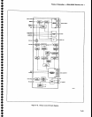
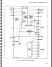
lC U2030
does five
things
(refer
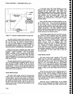
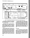
to Figure
7-15):
1.
Latch€s
the
current
numerator
in a
25-bit
latch
(25-to-1
data
concentrator)
and
latches
the
denomi-
nator in
a 17-bit
latch (17-to-1
data concentrator).
2.
Clears
the numerator
adder
circuits
(25-bit
sum-
mation
register).
3.
Performs
a
17-bit
priority
encode
on
the denomi-
nator and
loads
a
1
in
the appropriate
cell
of
the
25-bit
shift
register.
4.
Loads
the
latched
nurnerator
and
d€nominator
serially
into
the divide
circuit (subtractor)
using
the
contents
of
the
25-bit
shift
register
as a mask.
5. Clears
the
denominator
ripple counter
(1
Z-bit
counter)
to
zero.
Ten clock
periods
are
required
to
load
the numera-
tor
and
denominator
into
the
divide
circuit.
The
cycle
starts
on
a
SYNC
pulse.
The
lirst
bit
of
the
quotient
is
available shortly
aft€r
the first
clock
pulse
that follows
the
next
SYNC
pulse.
Division
is
performed
by
repeated
subtract and shift
operations.
Th€
quotient
is arrived
at
serially with
the most
significant
bit first.
Since onty
g-bit
accuracy is
required,
with
the
priority
encoder
output
used
as
a mask,
the
divider circuit
is loaded
with
the
g
most
significant
bits
of
the
denominator
and
the 16
most significant
bits
of
the numerator. (Ripple
borrow
for a
17-bit
by 25-bit
subtractor
woutd
be
so
tong
that
it
would be
impractical.)
The
peak
circuit
consists
of
a
peak
detector and
an
8-bit
peak
shift
register.
In operation,
the
previous
peak
Y
value from
the last
set
of samples
is
still
stored
in
the
peak
shift register
at
the start
of a conversion
cycle.
At
that time, the
peak
detector,
which is
a
serial
compare
circuit,
is set
to the state
that
qu€stions
whether
the
old
or
new number is
larger.
Each
bit
of
the
new
value
is
then
compared
with
the corresponding
bit
of
the old
value,
most significant
bit first.
When
one
value is
found
to
be
larger,
a flipJlop
is set
and
the smaller
number
is
gated
out
of
the
shilt
register.
The start
divide logic sig-
nal being
true then forces
the
peak
detector
to
select
7-42
the
new value and ignore
the
number
in
the
shift
regis-
ter.
The
peak/average
selector. a
multiplexer, selects
either
the
peak
or
average value
to b€
routed
to
the
memories
under
conrol
ot
the
PK/AVG
signal.
The
selector
output
is routed
through the Max Hold circuit.
which
functions
like
the
p€ak
detector.
When
the
MAX
HOLD signal
is
high,
the
value
that is routed
to
the out-
put
multiplexer is
the larger of
two
values:
the
current
memory
value
at
the
subject
X coordinate
or the
previously-selected
peak
or average
value.
Timing
to
set up the divide operation
and clear
the
numerator,
denominator,
and
peak
circuit
is controlled
by a 1O-stage
countEr. Taps are
taken
from
appropriate
sfages
to develop the
necessary clear
and
latch
timing
puls€s.
All
data
enters
and
leaves
th€
mgmory
serially. Data
read from
memory
enters an
8-bit shift register
and,
timed by
the
SYNC
signal,
is
transferred
to the
vertical
display output
latch
(display
register). The same
shift
register
is
used
for other
purposes,
so
the
DSPL
EN
(display
enable) signal
prevents
non-display information
from
being
transferred to the
output
latches.
An
exam-
ple
of
data
moving
through this
shift register
is sEen
in
the
B-Save A display mode. The A value is
first read
lrom
memory and
stored in
the
shift register. As
the
B
value
is read, the
subtraction is
done
serially
and
the
answ€r
is applied to the
shift register.
Since the sub-
traction must
be
perforrned
with
the
least signiticant
bit
first, a set of exclusive-OR
gates
change
the
order of
extracting B lrom
memory.
The shift register
direction
is
reversed
to
present
th€
most signiftcant
bit to
the
proper
display
latch. The shift
register output is also
applied
to the
output multiplexer.
In
subtraction,
the operation
performed
by
the
serial
calculator
is not
merely B minus A. The actual expres-
sion implemented is
(B-A)
+ K, where K is
a serial
input external
constant
specified
by the user.
This
per-
mits
zero to be
placed
anywhere
on
the
screen. To
avoid confusion
when
(B-A)
+ K results in an off-screen
position,
the subtractor blanks the
display.
(Ihe
sub-
tractor
examines the
carry
bit
and
borrow
bit
when
the
most
significant
bit
is calculated. lf either bit
is a 1,
the
screen is blanked.)
When
the Save
A mode is not selected
and
both
A
and B are
being
displayed,
maximum resolution
is
obtained
(1000
points
across
the display).
lf this display
includEs a very
narrow
pulse,
it is
possible
that
the top
of
the
pulse
is only
as wide as a single X coordinate.
lf
this maximum
value
were in
the
B Table and
the
Save
A
rnode was selected
and B turned
off,
there
would be
an
apparent
drop
in
amplitude. So,
when
the Save
A
mode
is selected, a special
set of circuits in
U2030
compares
all A and B values that
have
the
same X
value,
and
stores
the
larger
in Table A. The B value is
read
and


