


Theory
of
Operation
-
4g4A/4g4Ap
Service,
Vol.
1
Graphical
presentation
of mathematic
functions
or
experimental
data
is
common.
one
such
graph
has
a
single
Y value
for
each
X value.
An
alternaie
presenta_
tion
of
the
data in
this
graph
would
be a
table
simply
listing the
x coordinate
values
along
with a
correspond-
ing Y value
for
each
X value.
To
further
simpliiy
the
graph,
if
the first
X
value
and
the spacing
beiween
X
values
were
known (all
spaces
assumed
equal),
the
two-column
table could
be reduced
to
a single
column
with
the X value
implied
by
the
position
of
the
y
value
in
the
column.
This
is
the
essence
of
cligital storage
_
to
convert a
vertical
analog
voltagg
(y
coordinate
value)
to
a
biiary number
and
insert
that number
in
a stored
table. Th€ location
of
the
y
value
in
the table
is
deter-
mined
by the
analog
sweep
voltage (X
coordlnate
value)
binary
conversion.
Once
a s6t
of
binary
numbers
thai
rspresent
values
across
a waveform
is
stored
to cr€ate
a
table, the waveform
can
be
recreated
at
any
time
by
conversion
of
the
table
vatues
(y)
and
positions
(X)
baci<
to analog voltages
that
represent
amplitude
and
sweep
positions.
The
digital storage
system
uses
a Tabte
A and a
Table
B. Table
B is
updated
every
sweep.
Tabte
A
is
also changed
unless
the
Save
A
mode is
selected.
There are
500 A
values
and
500 B
values.
The
spacing
between values
is
the same
throughout
both
tables,
but
the
starting
point
for
Tabte
B
is shifted
stighfly
so
that
when
both tables
are
read,
thE readout
values
are
inter-
laced.
When
the
signals
are
recreated,
the contents
of
either Table
A
or
Table
B can
be
displayed,
or
both
tables A and
B can
be
displayed.
tf
both
Tables
A and
B
are
to be displayed,
and
thg
Save
A
mode is
selected.
the
contents
of
both Table
A and
Table
B are
drawn,
each
display in
its own
trace. lf
the Save A
mode
is not
selected,
the contents
of
both Table
A
and
Table
B are
displayed on
one
trace,
with
1000
value
positions
across
the screen.
A
third
trace option
is also
available.
In
the
B-Save
A mode,
the
displayed
values
are
those
that
r€sult
from
an
arithm€tic
op€ration
and
are
the
difference
between
the contents
of
Table
A and
Table
B
for each
X
value
of
anatog
sweep
voltage.
Since
a signal
waveform
is
continuous
and
a
table
has
discr€t€ X values,
an
algorithm
determines
the
y
value
to be stored
for
a
particular
X valus.
This
allows
the operator
to select
one
of
two methods
to
determine
Y values;
peak
or average.
The
y
analog
voltage
is con-
tinuously
sampled,
with
the
sampling
rate
dep€ndent
upon
sweep
speed.
For
each
X value,
there are
always
at least two samples,
and
there
may
be as many as
217
samples. From
this set
of
samples,
either
the largest
sample
value (peak
value)
or
the
mean
of all
the sam_
ples
(average
value)
can
be s€l€cted.
Selection
between
pgak
ancl
averag€
ls
controlled
by
the
front-panel
PEAK/AVERAGE
control,
which
sets
a
dc level
that is
eompared
with
the
analog
vertical
input
to
produce
the
PEAK/AVG
logic
signat.
When
the input
signat
is
below
7-40
the
level
selected
by
the
front-panel
control,
the
signal
is
averaged; when
the input
is above
that level,
the
peak
signal
is
displayed.
The
dc level
appears
on
the
display
as a
positionable
horizontal
line. This
line
is
created
when
the
dc
level is
switched
to
the
analog
output line
during
the
cursor cycle
by the
CURSOR logic
control
signal.
Superimposed on
the
cursor
line is
an
intensified
spot
called
the
update
marker,
which indicates
the X
value
at which
new
Y
values
are
being computed
for
display
update. The
update mark€r
is formed
when
the
analog
sw€ep input
is compared
to
the display analog
X
output.
When the
two
are
the same value,
the sweep
is
forced
to
pause,
which
increases
the
marker
intensity at
that
point.
Two custom
integrated
circuits
are
th€ heart
of the
digital storage circuits.
Th€ v€rtical
control
lC contains
the
vertical
acquisition
and
display logic,
peak
detec-
tion, signal
averaging, Z-Axis
blanking, and
special Y-
value
processing
circuits.
The horizontal
control
lC con-
tains
the
horizontal acquisition
address counter,
hor,
izontal
display counter, 10-bit
RAM address
multiplexer,
and
a
system
control
matrix.
Th6
other
digital storage
control
circuits
consist
of
two
8-bit digital-to-analog
converters,
two
1O-bit
digital-to'analog conv€rters,
one
10-bit
latch,
8K
bits of random
access memory,
and
various auxiliary circuits.
Timing is controlled
by
OZ
ctock
pulses
(at
1 MHz) from
the
Processor
board to
the Horizontal Digital
Storage
board.
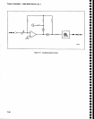
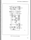
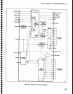
Vertical
Section
(Diagram
25)
The
Vertical Control lG
block
diagram
is shown in
Figure
7-15.
The
vertical
analog voltage
is converted
to
a Y
binary value by
an
8-bit
successive
approximation
register. Nine clock cycles
are required
for each Y
conversion.
After
the conversion
has
taken
place,
the
successive
approximation register
produces
the
negative-going
SYNC
signal.
Most functions
on both
th€ vertical and
horizontal
control
lCs arE synchronized
by
this signal. On the negative-going
transition
of
SYNC, the successive
approximation
register is reset to
10
00 00
00
(binary)
and
the
next conversion
cycle
begins. Incoming data
bits
ar€ latched into
the
register
on
th€
negative-going clock
transition.
From
the
regis-
ter, the
output
data
is applied
to the
peak
and
the
averaging
circuits.
The averaging
circuit
consists
of
three
groups
of
cir-
cuits;
those that
accumulate
all
the
Y values for a
given
X value into
a
grand
total
(called
the
numerator),
thos€
that
count
the
number of samples
that
make
up the
numerator (this
total is called
the denominator),
and
those
that subtract
and shift
to divide.
o
o
I
o
a
o
t
o
o
o
o
o
I
I
o
t
o
t
e
I
a
o
I
a
o
o
o
o
t
o
o
o
o
o
I
o
I
C
I
o
t
T
o
I