


Theory
of
Operation
-
49{A/4g4Ap
Service,
Vol. I
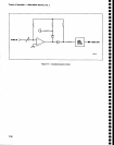
The
output
of
u3038A is
apptied
through
edge
con-
nector
pin
BB
to the
gain
control
plN
diode
in the Band
Leveling
circuit.
For example;
when
band 1
is
selected
(U3023 pin
1 low),
current
through
Band
1
Gain
poten-
tiometer,
R2031,
and the emitter
of
e3036
sets the vol-
tage
through R2033
to the
summing
input
of
operational
amplifier
U3038A.
The
increas€d
output
of
U303gA
increases
the current
through
band
levEling
plN
diode
CR2021 and
increases
the
gain
of
the
stage
according
to the setting
of
Band
1
Gain
pot€ntiometer
R2031.
In
similar
fashaon,
the
other
potentiometers
(R9034,
R3030,
R3019,3A22,R3024,
R3026,
R3032,
R302g,
and
R3028)
allow
adjustment
of
the current
for
each of
the
other
bands.
An additional
diode
may
be added
to
each
decoder
output,
for
bands
4
through
10,
to
transmit
the
low.
via
edge
connector
pin
OD,
to the
gain
control
transistor,
in
the
Band
Leveling
circuit,
and
increase
the
gain
more
lor
these
bands. These
diodes
are
CR3022,
CR3O23,
CR3024,
CR3025,
CR3031,
CRg027,
and
CR3026. tf
needed
these
diodes
are
installed
during
instrument
calibration.
The
+5
V regulator
circuit,
U9041, supplies
a
noise-
free
+5 V source
for
the VR
system.
This
ls required
because of
noise
in
the
+5
V
main
supply.
2nd
Filter
Select
Circuits
(Diagram
2l)
Circuits on
the
2nd Fitter
Setect
board
(46gAg)
operate
in conjunction
with
the circuits
on
the lst
Filter
Select board
(A68A4)
to set
the overall
systern
bandwidth. Banks
ol
filters
are
select€d
under
the mas-
ter microcomput€r
control.
Data
bits
0, 1,
and 2, lrom
the
data
bus, are
applied
to decimal
decoder
U9070
(which
outputs
a
low
on
th€
appropriate
output
pin
to
enable
th€ selected
filter).
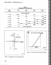
Bandwidth
selections
are
10 Hz
to
1 MHz
in
decade steps,
plus
3
MHz.
Filter
selection
is
accomplished
as
previously
described
for
the 1st
Filter
Select circuit
except for
the
3 MHz,
1 MHz,
and
100 Hzl10
Hz
selections.
The
input
signal,
from
the
Band
Leveling
circuit via
jumper
EE, is
routed
through
the selected
filter to
the
Post
VR Amplifier
circuit,
via
jumper
JJ.
Nominal loss
through
the
filter
circuit
is approximately
12dB, with
internal
adiustment
compensation
for
variations
between
the filters.
The
output
level
is
nominally
-12
dBm.
The filter
for
each
bandwidth ranges
lrom
no
filter
at
all
to
a
temperature compensated
crystal
filter. An
important
difference
between
the i st
and
2nd filter
select
circuits
is
the
addition
of a
gain
adjustment
in
all
except
the 100
kHz
circuit.
This
adjusts
the amount of
att€nuation
through
the
other
filters
and
matches
the
output
level
to
that
of
the 100
kHz filter.
since
the
Band
7-28
Leveling circuit furnishes
compensation
gain
to obtain
equal
signal levels for all
bands,
this adjustment
com-
pensates
for
variations
between the filters.
The 3 MHz
and
1
MHz
bandwidth
signals
use
the
same
path
through this
board.
No filter is
required
here,
becauso
of filtering
in
previous
stages.
When
€ither
3
MHz or 1
MHz
is
selected,
the signal
goes
through
a
simple attenuator
with a
gain
control
for
matching levels with
th€
other
sections. Pins
2 and
9 of
U3070 are tied
together to
select
the
3
MHz/l
MHz
path
for either
bandwidth.
The 100
kHz filter is a
double-tuned
LC
circuit
designed for a
good
tima-domain response shape.
The
filter is
tuned
with
composite variable capacitors
con-
sisting
of
small air
variables
paralleled
with
switched
fixed capacitors. A
third
variable capacitor
may
be
adiusted
lo
establish
the
desired bandwidth. For
Option
07 instruments, a similar
300 kHz
filter
replaces
the
100 kHz filter.
The 10
kHz
filter
uses
a
two-pole monolithic crystal
filter. The
impedances
at
the input
and
output are
matched
to
50
ohm
by
T5047 and T7050. An attenuator
that
contains
Gain
adjustment
R3039 is included at
the
filter input
for
filter variation compensation.
The
1
kHz filter
is also a
two-pole
monolithic
crystal
with impedance matching
transformers
T40/,4 and
T:7043. A Gain
adjustment
is
also
part
of
th€
attenua-
tor.
The
100 Hzll0 Hz
filter is
a
temperature-
comp€nsated high-Q crystal
filtsr. The actual filter
bandwidth
is about
200 Hz. This filter augments
the
filter in
the
1st Filter
Select
circuit
and
reduces noise
produced
in
the
intervening stages.
Freq
Adjust R4025,
in a
voltage
divider
circuit,
sets
the
center frequency of
th€
crystal filter.
The 100Hzl10Hz
path
is selected
by Q2020
and
08035
through
diodes cRl017
and cR8016 on
the
input
and output
respectively.
when 10
Hz
is
selected,
pin
7
of
U3070
goes
low
turning
on
Q2020
and
Q8035.
When
100H2 is selected,
pin
6
of
U3070
fonarard
biases
cR3068, thus
enabling
the
path.
Gain
control
R3015 adjusts
the
100
Hz level.
The
10
Hz level is
set by
a control on
the
10
dB Gain Steps
board
(A68A5),
as
previously
described.
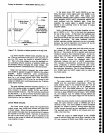
Post VR
Amplifier
Circuit
(Diagram
21)
The Post
VR
Amplifier
circuit
provides
the
final
VFt
system
gain
to bring the signal
to the
requir€d
+6
dBm
output
level
and
provides
the
final
band-pass
filtering.
The
circuit consists of
two
stag€s of
gain
followed by
a
filter.
o
o
a
o
'o
I
o
o
o
o
o
I
I
o
o
o
o
I
o
o
o
a
t
o
a
a
o
O
o
t
o
a
o
o
I
I
o
a
o
o
o
I
o
a