


Theory of
Operaton
-
4g4[l4g4Ap
Servtce,
Vot. 1
appropriate
action.
Th€
following
is
a
description
of
the
hardware and
a
brief
description
of
the software
used
bythe
front
panel
CPU.
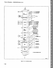
Potentiometers.
The
following
controls
or
adjust-
ments
generate
analog
signals
used
by other
functions
of
the instrument.
These
controls
are
non-
programmable.
INTENSITY
is an input
to th€
Z-Axis/RF
Interface
board
to
control
trace brightness.
PEAK/AVERAGE
is
a
digitat
storage
input
that
causes
signals
to
be
either
peak
detected
above
or
averaged
below
a
displayed
cursor
lane
that
tracks
this
control.
MANUAL
SCAN
sweeps
the
spectrum
or
display in
manual
sweep
mode.
POSITION
centers
the
horizontal
and
vertical
deflection
on
the crt.
LOG/AMPL
CAL
varies
the
video
signal
level
prior
to the Video Processor
board
and
adjusts
10
MHz lF
gain
to calibrate
the
log
display.
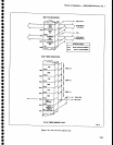
OuFut
Mode
Shift Registers
and
LED'.
As
previ-
ously
described,
LEDs
mounted
behind
a
pushbutton
or
below front-panel
labels
indicate
the
mod€ of
operation.
Some versions
of
the
spectrum
analyzer
may
not
use
all
indicators; for example,
the non-programmable
versions
do
not have a RESET
TO
LOCAL
button,
The
LEDs
are
driven
by shift
registers (U5O4S,
U6081,
U6028,
U6045.
and
U1049)
that
reside at
address
74
(hex)
on
the instrument
bus. The
shift
regis-
t€rs that drive
the
LEDs
are
reloaded
each
time
a
LED
changes
state.
The
master
microprocessor
changes
the
appropriate
bit in
the
LED code
then reloads
all
registers.
The
shift register
U60gl
that
drives
the
GRAT ILLUM
LED also
controls
the voltage
regulator
U6090,
which
provides
power
for
the
graiicule-lights,
DSl0t1
and DSl013.
Proeessor.
The
CPU is an
874i self-contained
g-bit
microprocessor
with
on-chip
EPROM
and RAM.
Refer
to Intel
UPI Users
manual
for a complete
description
of
the this microprocessor (lntel
8741).
The
lC has
a self-contained
clock
and
a
timer.
The
clock
uses
a
6
MHz crystal,
y3030,
as
the
resonator.
The timer functions
either
as
a
programmable
timer
or
counter.
7-98
The CPU
has
two input/output
ports.
Port
plGplT
is input
only
and
P20-P27
in
an input/output
port.
Each
port
is
8-bits wide.
In
addition,
the
CPU has
an
8-bit
data
port
(D0-D7)
called
the
output
buffer, which
tatks
to
the master
microprocessor. In this
application
all
data
is
output only with
U4030 being a
buffer between
lhe
GPU
and
the instrurnent
bus.
Infoffnation
that the
cPU
wishes
to
relay
to the master microprocessor,
is loaded
into
a
latch
connected
to the
output
buffer
U4030. The
master
microprocessor
accesses
the
CPU by
pulling
address
F4, out of
decoder U6024, low
to activate
the
output
bufier and enable
U4030
so
data
is
passed
onto
the instrument
bus.
The
CPU is reset
by the master
microprocessor.
When DB3 is
selected for
more
than
10 ms
(same
as
writing
08
at
address 74)
C1016 charges
and
U1024A
output
resets
the CPU.
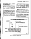
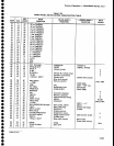
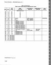
Scanning the
Keyboard. The
front-panel
keyboard
is
arranged in a matrix of 4 rows
of
I
columns
and
6
rows of
7 columns
(see
Table
7-24). The
RESOLUTION
BANDWTDTH,
SPAN/D|V, T|ME/D|V,
MIN
RF
ATTEN
dB,
and REFERENCE
LEVEL selectors
are
rotary switches where
each contact occupies
a
position
in
the
keyboard switch matrix.
The TIME/D|V and
MIN
RF
ATTEN a(e
position
dependent. The master
microprocessor
notes
the
current s€tting of
these
selec-
tors
by
noting which contacts
are
closed.
When
a
change is made
the
master
microprocessor
notes which
direction the
selector was
moved
by
noting
the
relative
position
of
the current contact
closure
with
the
previous
setting.
Pull
up
resistors, within
R2041
plus
R2044, on
each column of
the
row currently
being
read,
will
pull
that column high
if
the switch is
open.
The
basic
algo-
rithm
of scanning is
to
pull
one row at
a time
down
and
note which columns have
a 1 or
0.
Port one.
Pl
0-P17
(pins
27€4), read the
columns. Part
of
port
two
(pins
21-241 are responsible
for
activating
the
rows.
Basically
the
process
consist of
pulling
one
row at a
time down
to E logic 0
and
then reading all the
columns. lt
a
switch contact
is
open
it reads
a
"1
"
and if it is closed it
reads
a
"0'.
Since
there
are 10 rows
to scan
and only
4
pins
(P2O-P231available
at
the
number
2
port,
the
output
is
multiplexed
through U4021
and
U5021.
These lC's are
open
collector
output, TTL compatible
multiplexers.
They
decode data
out of P2O, P21, P22, and P23
(pins
21-241
and
their
output
pulls
the
appropriate row of
keys
down.
Due to
the
characteristics
of
the
switch
matrix. if
two keys,
in
any
row or column are closed, and
a third
is
closed
so
three
corners of
a
rectangle are
esta-
blished in the key matrix,
the
CPU will
see a
phantom
closure
at
the
fourth corner. For example;
if
Y6/X3,
Y6/X7
are
closed, and
then
Y3lX7
is closed,
the
CPU
o
o
o
o
o
o
o
a
o
a
I
o
t
)
t
o
o
o
o
o
o
O
o
o
I
I
o
o
a
o
o
o
a
o
O
I
a
a
I
o
o
a
o
o