


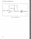
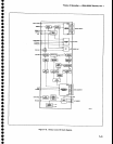
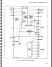
The
filter
consists
of
resistors
R2O2g,
RZOZ1,
R2022
and
capacitors
C3026
and
C2016,
"onn""t"O
between
U3062
and
U2066.
Tabte
7-6
lists
itre
tiiiei
components
in
thE
circuit
for
each
of
the
six
OanOwiOttrs.
Data
bits
2,
1:
"1!
4
are
apptied
to
switch
U2O15B
(pi-ns
B, 16,
and
9)
which
selects
the
components.
frorir
U2OOOB,
the
signal
is
routed
through
contacts
Z
ana
6 of
switch
!9.qpp
to. edge
connector
pin
57
as
th€
VtoEO
FILTER
OUT
signal.
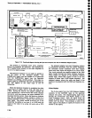
Video
Blanking
The
video
btanking
circuits
allow
selective
blanking
9l_!h"
lower
and
upper
ends
of
the
locat
osciilator
range.
Selective
blanking
is
required
because
the
local
oscillatgr
sw€eps
the fuli
span-regardless
ot
the
band
IT,r-.:,].P.,:9:?
s_y:tem
is
desisn;c
to
"tr""tiu"ry
op"n
a.otsptay
window
only
during
the
time
for
display.
Data
bits
5,
6, and
7,
under
coritrol
of
the
-*iiro"orput"r,
select
the appropriate
amosnt
of
display
for
eacn
end.
.
Video
blanking
and
the
PRESELECTOR
DRTVE
sig_
nal (which
provides
frequency
information,
in
voltag-e
rorm)
are
located
on
the
ViOeo
processor
board.
::1,:h_
yg.0g3.
incorporates
a
disabte
function
rhat,
wnen provicted
a
tow
input,
opens
all
switch
s€ctions
regardless
of
individual
section
input.
This
feature
allows
the
VTDEO
FTLTER
OUT
signat
to
be
easity
blanked
at
wiil.
The
disable
function
is
controlled
by
a
combination
of
outputs
from
comparators
U30154
anO
UgolsB.
I11ttlq.these
comparators
are
from
the
PRESELEC_
TOR.
DRIVE
signal
and
a
combination
of
vottage
divid-
ers
that
are
switch
selected
under
control
of
dai=a
bits
5,
5,
and
7.
The
PRESELECT_OR
DRTVE
signat
is applied
from
edge
connector
pin
54
through
OiiiJer
resistors
R4013
and
R4012
to
the
inverting
iriput
oi
UgOtSR,
anO
through
divider
resistors
R4014
inO'Ra0tito
the
non_
inverting
input
of
U3O15B.
These
dividers
rectuce
the
excursion
of
the drivE.signal
from
(+10V
to
_10V)
to
(2.5
V
to
-2.S
V),
which
is
the
maxlmum
input
tevet
to
the
comparators.
Input
to
the
non-inverting
input
of
U3015A
is
from
divider
resistors
R9011,
RgOl
d
and
selected
r€sistor
R4015.
The
inctusion
of
R4015
is
controlted
by DB7
through pins
2 and
3 of
U9025.
The
junction
of
divider
resistors
R3011
and
Rg0l2
is
connected
to
ground
through
R401S
for
band
2.
Input
to
the
inverting
input
of
Ug01
58
is
from
divider
resistors
R4018,
R4012,
and
selected
resistor
RgO2g.
The
inclusion
of
83023
is
controlleO
Oy
OeO
through
pins
10 and
tl
of
U3025.
The
junction
oi
Rg0t
anO
R3012
is
connected
to
+S
V
ttrr6ugn
RO0rS
when
it
is
selected.
This
switching
arrangement
of
negative
and
positive
levels
for
comparisbn
with
the
reduced
PRESELECTOR
DRIVE
signat
enabtes
the
iop and
bot_
Theory
of
Operation
-
494Al4g4Ap
Service,
Vot.
i
tom
extr€mes
of
the frequency
excursion
to
be
blanked.
The
blanking
is
activated
by the
disable
function
of
switch
U3063,
which
is controlled
by
the
microcom-
puter.
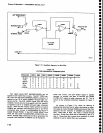
DlclTAL
STORAGE
(Diagrams
25
and
26)
The
Digitat
Storage
circuits
provide
the
abitity
to
store
and
process
a signal
before
displaying
it.
fnis
allows
flicker-free
displays,
Even
at
tire'stow
swesp
rates
required
for
narrow
resolution
bandwidth
meaj-
urements.
Digitizing
the signal
also
allows
signal pro-
cessing
and
marker generation.
.- -
Th-"
processing
includes
detecting
peak
amplitudes
(Max.Hold),
storing
a
signat (Save
A),'subtracting
one
signal
from
another
(B-Save
A),
signal
averiging
(Averaging),
and
signal
comparison
(View
A anO
Vei
g)t
These
operations
use
two
memory
banks
to
independently
store
two complete
signals
tirat
are
Each
digitized
at
500
points
across
the
lweep.
Therefore,
two signals
may
be observed
simultaneousty
or
pro-
cessed
in
separate
ways.
The
markers
are
used in
a
variety
of ways.
There
ar€
two
waveform
markers
that
th€
user sets
for
vari-
ous
measurements.
In
addition,
an
update
mad<er
shows
where
the
actual
sweep
is with
reierence
to
the
refreshed
display.l
Four
instrument
bus
addresses
are
associatgd
with
Digital
Storage.
Addresses
7A
and
lB
are
write
addresses.
FA
and
FB
are
read.
These
addresses
are
shared
by
both
the
Horizontal
and
Vertical
Digital
Storage
circuits.
Logic on
the Horizontal
Oilitat
Storage
board
controls
which
set is
activo.
7A
onlne
Horizontal
Digital
Storaga
board is
further
subdivideO
into
I subaddresses
by 3 bits
in address
ZB
on
that
board.
Address
tables
in
the
circuit
descriptions
for
the
appropriate
boards
show
details
of
the Digital
Storage
addresses
In
the
Max
Hold
mode,
the highest
amplitude
at
each
of
the 1000
points
in
successive
sweeps
is
stored
and
displayed.
ln
the
Save A
mod€,
a signal
is
stored
in
one
memory
for
later
examination,
and
is
not
updated.
In
the B-Save
A mode,
the A
signal
is stored
and
not
updated,
then
arithmeticaily
subtracted
from
the B
sig_
nal,
which
is
stored,
but continually
updated. tn
ttre
averaging
mode,
the
display
area
is
divided
by a
hor_
izontal
cursor.
Signals
above
the
cursor
are
peak
cletect€d
and
displayed,
and
signals
below
the
curcor
are
averaged.
ln
the
View
A
and View
B
modes,
the
contents
of
the
selected
memory
or
memories
are
displayed.
_89t9_are
als"-rid*
rnarkers
lhat
may
be
fed
to the ,ear-panel
MA8KER
I
VIDEO
input
These video
mdrkers
are
from
an exliernal
source,
and
are not
part
of
the
digital
storage
system.
See
the
vroeo
processor
description
for
more
informaiion
about the video
matkers.
7-39